Al-Doping Effect on the Surface Morphology of ZnO Films Grown by Reactive RF Magnetron Sputtering ()
1. Introduction
Owing to the high natural abundance of zinc, and to the low toxicity, high optical transmittance, low electrical resistivity and optical gap of about 3.3 eV, zinc oxide (ZnO) thin films have been widely studied for applications such as transparent conductive oxides (TCOs) [1]. Nowadays, indium tin oxide (ITO) is one of the TCOs that are mostly used in optoelectronic devices, but it has some disadvantages. The main one is that the chemical element indium which is the main component of ITO is scarce in nature. Consequently ITO has a high production cost [1,2]. Therefore, ZnO is a promising candidate to replace ITO and can be used in various applications such as OLED (organic light emitting diode) displays, smart windows, solar cells, etc. [1,3,4].
Thin ZnO films have been produced using a variety of techniques such as chemical vapor deposition (CVD) [5], plasma enhanced chemical vapor deposition (PECVD) [6], laser ablation [7], sol-gel [8], spray pyrolysis [9], magnetron sputtering [10,11] and atomic layer deposition [12]. The high deposition rates and the possible synthesis on large substrates (essential for large-scale synthesis) make magnetron sputtering particularly interesting, especially since it may be employed at low temperatures (including room temperature).
Many factors strongly influence both the physical and chemical properties of ZnO films, such as the type of doping, film thickness, substrate type and the growth temperature. Recently, the influence of the Al doping concentrations on the optical and electrical properties of ZnO:Al films has been studied [3,13,14]. More recently, several studies have focused on the influence of doping levels on the surface morphology of the films [4,15]. In the present work intrinsic and (slightly) aluminum-doped ZnO thin films were synthesized by reactive RF magnetron sputtering to investigate the influence of the Al content, principally on the structural and surface morphology.
2. Experimental Details
The pure and Al-doped ZnO thin films were deposited onto silicon and glass substrates by reactive RF magnetron sputtering using a zinc-aluminum (0.5 wt%) target of 99.99% purity. Depositions were performed simultaneously on 1 mm-thick glass plates and 375 mm-thick type N (100) silicon substrates, of electrical resistivity 100 Ωcm. Oxygen gas was used as a VI precursor source, whose flow rate was controlled using a needle valve and a flowmeter (MKS 1179A). The pressure inside the reactor was monitored using a Pirani gauge (Kurt J. Lesker 945). The plasma was excited using a 13.56 MHz radio frequency (RF) source (with impedance matching, Tokyo Hy-Power Labs). For both depositions the ratio of the partial pressure of oxygen to argon was set at 1:10 and the total pressure was held at 1.4 Pa. The pure and Al-doped ZnO films were deposited at the same growth rate (R = 12.5 nm/min.) for 60 minutes. To keep the growth rate constant, the RF power was 85 W and 100 W, respectively. The substrate temperature was maintained at 100˚C and the target-substrate separation was set at 50 mm.
XRD measurements of the films were conducted using an X-ray diffractometer (Rigaku Model D/MAX- 2100DC) with Cu Kα radiation of wavelength (λ) 1.5405 Å. The surface morphology was investigated using an atomic force microscope (AFM, XE-100-Park Systems). The scanned area was 2 μm × 2 μm with 512 × 512 pixels. The optical transmittance of the films was obtained using a UV-Vis-NIR Lambda 750 (Perkin Elmer) spectrophotometer. The chemical composition of the films was examined using energy dispersive spectroscopy (EDS) with a scanning electron microscope (SEM, Quanta Inspect S-FEI Company).
3. Results and Discussion
3.1. UV-vis-NIR Analysis
Figure 1 shows the optical transmittance spectra obtained for the pure and Al-doped ZnO films deposited onto glass substrates. The optical transmittance of the films was obtained by averaging in the range 450 - 650 nm, as indicated by the vertical dashed lines. In the visible region both films had an optical transmittance of greater than 80%.
In addition, one can see that the absorption band of the Al-doped film shifts to lower wavelengths, i.e. there is an increase in the optical band gap of the film. The optical energy gap can be determined using Equation (1), which relates the absorption coefficient ( ) and the gap energy (
 ) [15]. From Figure 2 it is possible to determine the energy gap by extrapolating the linear position of the graph to the point where the absorption coefficient is zero, since at this point
 .
.
 (1)
(1)
where  is the photon energy,
  is the optical gap energy for direct allowed transitions and B is a constant dependent on the refractive index of the material, the electron effective mass and the speed of light in vacuum.
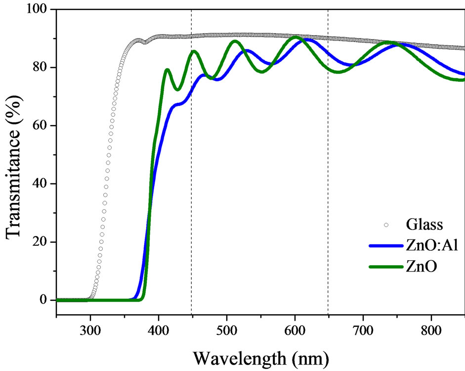
Figure 1. UV-visible optical transmittance spectra for the ZnO and ZnO:Al films deposited onto glass substrates. For comparison, the optical spectrum of a glass substrate is shown.

Figure 2. Plots of (αE)2 vs. photon energy (E), for ZnO and ZnO:Al films deposited onto glass substrates.
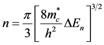
The optical gap energy of the pure ZnO film is about 3.28 eV and increased to 3.36 eV when the film was doped with aluminum. This increase is related to the Moss Burstein effect, which causes the Fermi level to move into the conduction band states, filling the lower conduction band levels and hence requiring more energy to promote an electron from the valence band to the conduction band [1]. The shift in the Fermi level is given as a function of carrier density (n), the effective conduction mass ( ) and the change in gap energy (
 ) by Equation (2) [1].
 (2)
(2)
where h is Planck’s constant. For ZnO  is equal to 0.38 [16]. Normally, for the intrinsic ZnO films, the carrier density is found to be ~ 5.9 × 1018 cm−3 [16]. As, in this case of aluminum doping
  = 8 meV, the density of carriers increases to about 2.6 × 1019 cm−3.
3.2. EDS Analysis
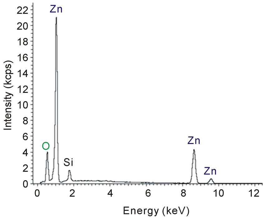
The chemical composition of ZnO and ZnO:Al films deposited onto silicon substrates was investigated using EDS. In Figure 3(a) it is possible to observe the spectrum of the ZnO film, where the intensities of the peaks of the elements zinc and oxygen are consistent with the concentrations in the film. Similar zinc and oxygen peaks are also observed in the spectrum of Figure 3(b), but a small peak, which corresponds to aluminum, is also clearly observed. This result is expected since the ZnO film was doped from a metallic zinc target with 0.5 wt% of Al. It is also possible to infer the presence of silicon from the two spectra of Figure 3, which is probably due to the substrate, since the ZnO films are < 1 µm thick and during scanning the electron beam can reach the substrate. These results are in agreement with other studies [9,17].
Furthermore, semi-quantitative calculations based on the EDS spectra show that the aluminum concentration in the ZnO:Al film is 0.9 at%. In the ZnO film, the Al concentration detected is less than 0.02 at%. This value is consistent with the aluminum concentration in the metallic target and the low concentration of charge carriers, calculated from the optical gap. Thus, the ZnO:Al film may considered to be slightly doped. Despite the low concentration of Al, however, the presence of aluminum atoms is sufficient to interfere with the growth dynamics of the film. As discussed below, with Al doping the surface morphology and crystal structure are remarkable changed.
3.3. XRD Analysis
The crystallinity of pure and Al-doped ZnO films was investigated using XRD. Figure 4 shows spectra of the ZnO and ZnO:Al films. These X-ray diffraction spectra show that both films are polycrystalline and have a preferred crystallographic orientation in the (002) plane along the c-axis perpendicular to the substrate surface. The peaks of the spectra correspond to the wurtzite structure of ZnO. The identification of the crystal phase was performed using data from the standard table of ZnO (JCPDS 65-3411).
The mean grain size ( ) was determined using the Scherrer formula [17], Equation (3).
 (3)
(3)
where K represents a shape factor, that normally has a value of 0.9 [17],  is the wavelength of the X-rays,
 (a)
(a)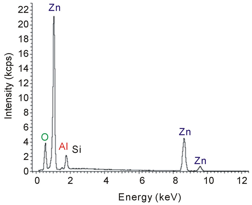 (b)
(b)
Figure 3. (a) Spectrum of a ZnO film deposited onto a silicon substrate. (b) Spectrum of an Al-doped ZnO film deposited onto a silicon substrate.
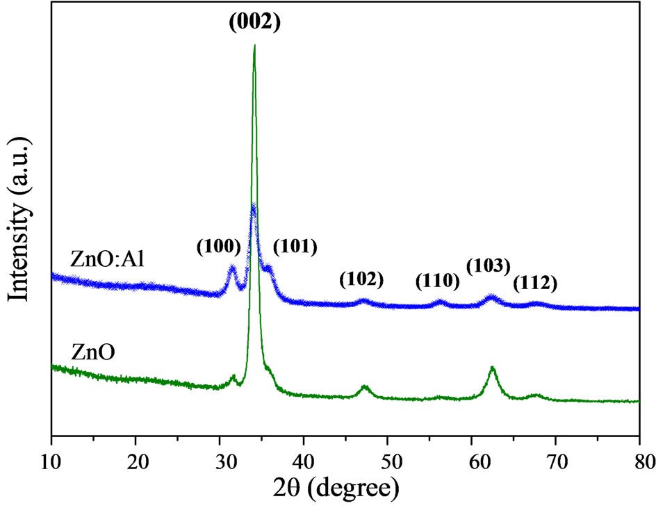
Figure 4. XRD spectra of pure ZnO and ZnO:Al films deposited onto glass substrates.
 is the value of the Full Width at Half Maximum (FWHM) of the (002) X-ray diffraction peak and
  corresponds to the Bragg angle. The pure ZnO film has a grain size of 10.7 nm. When the film was doped, however, the grain size decreased to 6.1 nm.
It can be seen that for the ZnO:Al film the (002) peak has a lower intensity (1700 a.u.) compared with that of the ZnO film (5700 a.u.), indicating a degradation of the crystalline structure of the ZnO film when slightly doped with aluminum. In the diffraction spectra there is a shift in the (002) plane to smaller angles (θ = 34.13˚) compared to the standard angle given in the JCPDS table (34.43˚). This indicates a compressive residual stress in the ZnO film. It is also observed that the FWHM of the peak is mainly influenced by grain size, stress and crystal imperfections, therefore, the FWHM values can be used as a negative indicator of film quality. For the film of ZnO and ZnO:Al, FWHM values are approximately 0.76˚ and 1.37˚, respectively. This increased FWHM indicates that the quality of the film decreased with slight incorporation of Al in the film [17]. These results show that the incorporation of Al in the film chiefly influences the dynamics of grain growth, i.e. diffusion of material between the grains. The explanation of this may be that aluminum causes defects in the crystal lattice of the film, which hinders grain formation [17].
3.4. AFM Analysis
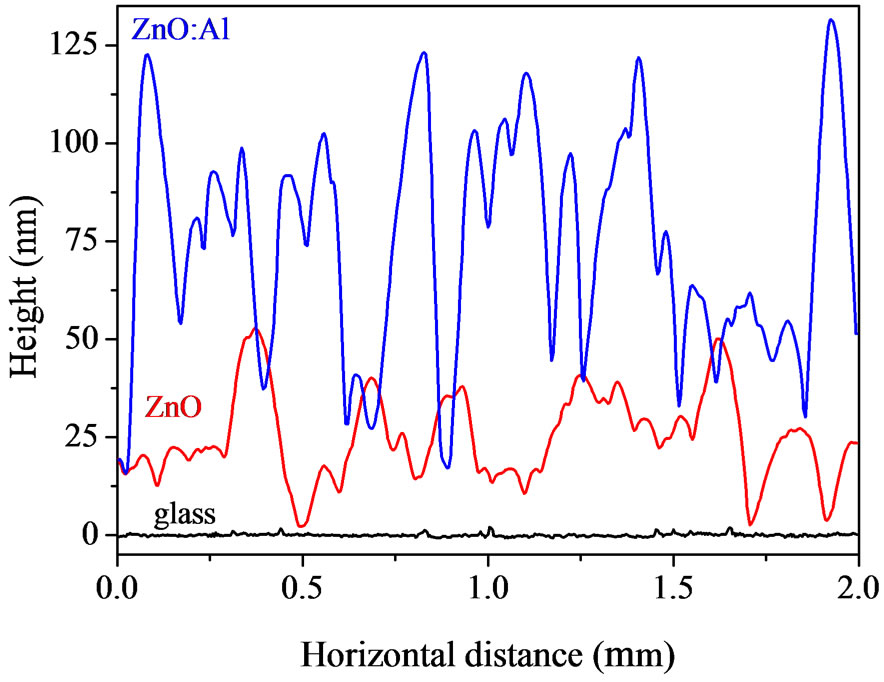
Figure 5 shows 2 μm × 2 μm AFM images obtained for the pure and Al-doped ZnO films deposited onto glass and silicon substrates, respectively. Although each film exhibits a homogeneous distribution of grains, there is a visible change in the morphology of the films when they were doped with aluminum. To better visualize the surface morphology of the films from the AFM images shown in Figure 5, Figure 6 shows lateral profiles of ZnO and ZnO:Al. It can be observed from both figures that films doped with Al show a greater vertical grainsize compared to those of pure ZnO.
The surface roughness (rms) of pure and Al-doped ZnO films, and of the substrates, were obtained from the 2 μm × 2 μm AFM images and are presented in Table 1. The pure ZnO film deposited onto glass showed a surface
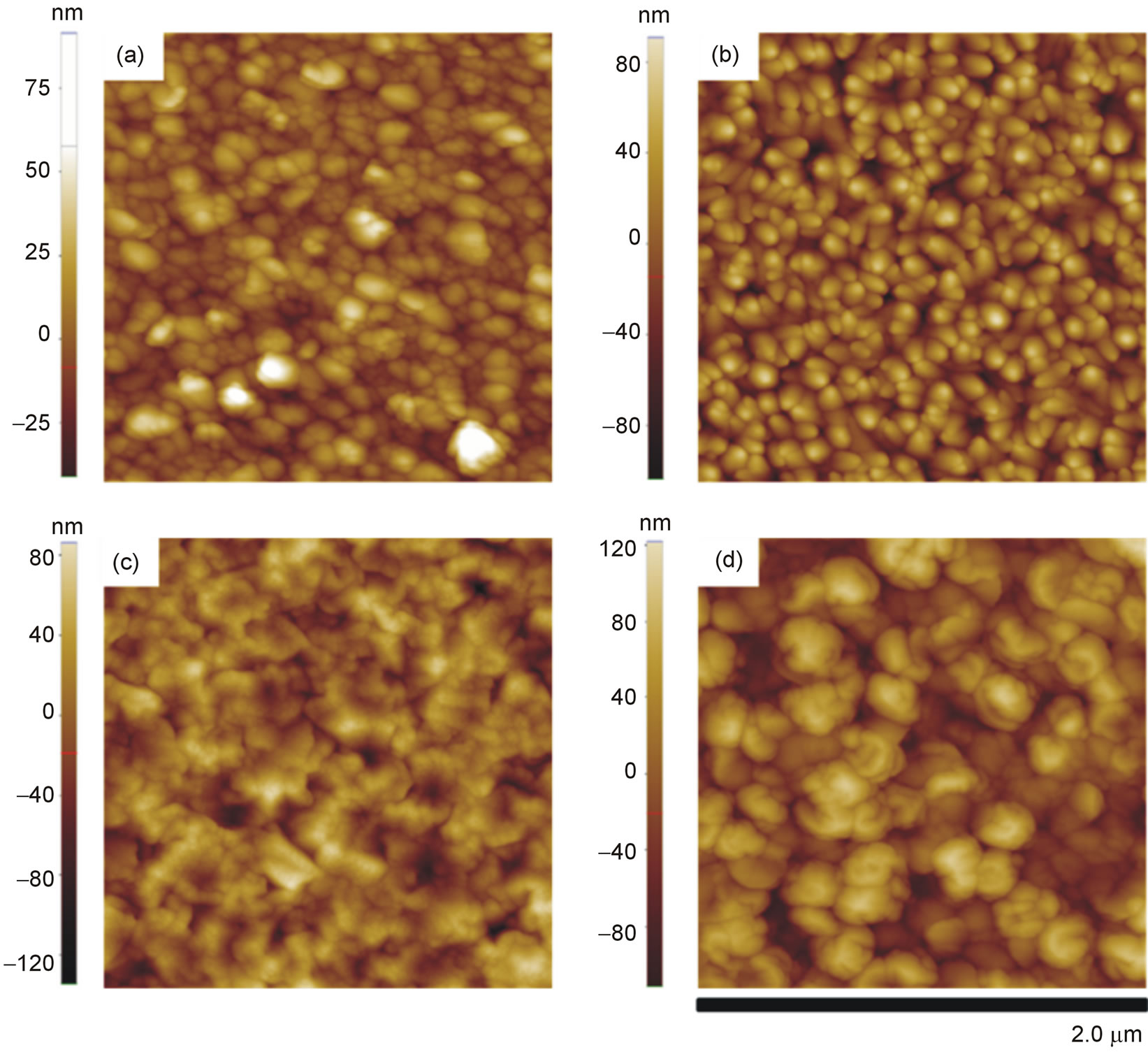
Figure 5. AFM images (2 μm × 2 μm) of ZnO and ZnO:Al films deposited onto glass and silicon substrates. (a) ZnO (glass), (b) ZnO:Al (glass), (c) ZnO (Si) and (d) ZnO:Al (Si).
 (a)
(a)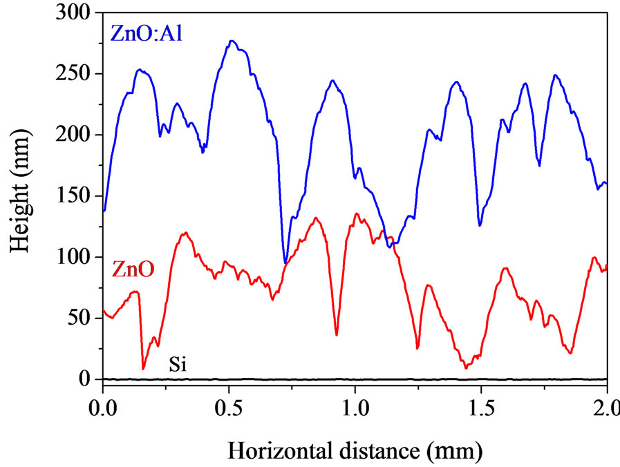 (b)
(b)
Figure 6. AFM profiles of 2 μm obtained by lateral scanning of ZnO and ZnO:Al films deposited onto glass (a) and silicon (b) substrates. To avoid superposition the profiles have been shifted vertically.
roughness of ~ 14 nm. For the film of ZnO doped with Al, however, there was an increase in roughness to ~ 28 nm. The same behavior was observed for the ZnO films deposited onto silicon substrates. The roughness of the pure ZnO film was ~ 28 nm and increased to ~ 40 nm when the film was doped with Al. Surface roughness increases with increasing Al concentration in ZnO as described in other studies [4,15]. The kinetic mechanism responsible for this is taken to be a decrease in surface diffusion [18]. On the other hand, the lateral grain size is not systematically altered by the introduction of Al. In a similar way, Hasuike et al. [3] show that when the concentration of Al is increased from 0 to 2.9% in ZnO films grown by reactive DC magnetron sputtering, the grain size increases slightly. In our case, according to Table 1, it may be observed that the lateral size of the grains of the ZnO:Al/glass film decreases compared to that of the ZnO/glass film, making them thinner (Figure 6(a)). Considering growth dynamics, these results may indicate that aluminum doping reduces adatom diffusion between adjacent crystalline grains. Consequently, the films tend to be rougher, as discussed by Kajykawa [18], but with the lateral size only slightly changed.
The films deposited onto silicon substrates showed a different surface morphology, however, with larger grain structures and undefined shapes. In topographical terms, both substrates exhibit surface roughnesses (rms) below 0.5 nm. Therefore, it is likely that areas with epitaxial growth on the silicon substrate have influenced the formation of wider grains of ZnO and ZnO:Al, even when the substrate temperature was kept at 100˚C, as shown in Figure 6(b). In this case, the influence of the substrate was stronger than the influence of the dopant on the formation of grain structure. As revealed by the data of Table 1, the lateral grain size was greater in the ZnO:Al/Si film compared to that of the ZnO:Al/glass film. Kajikawa
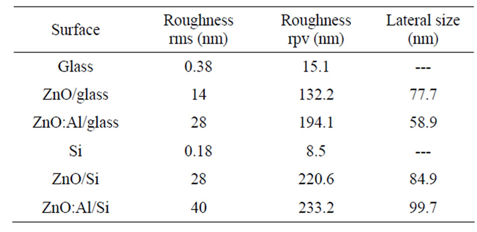
Table 1. Surface roughness rms (root mean square), rpv (roughness peak to valley) and lateral size of surface structures measured using AFM on samples of ZnO and ZnO:Al on glass and silicon substrates.
et al. reported that the initial nucleation of polycrystalline films can depend on the type of substrate, and that the film growth can be epitaxial or non-epitaxial, which consequently influences the final morphology of the films [18].
In fact, the influence of substrate type has been reported in the literature, at least for higher growth temperatures [19,20]. Liu et al. showed that for deposition at 400˚C, the structure of ZnO/GaAs (001) has smaller grains than those seen for ZnO/c-sapphire grown simultaneously [19]. Actually Wang et al. showed that there are morphological differences amongst ZnO:Al deposited onto glass substrates, polyamide and stainless steel at 300˚C [20]. In this case, the surface roughness increased and grain size decreased compared to values seen for films deposited on stainless steel. In both cases, the effect is due to the difference in lattice parameter between the substrate and film.
4. Conclusion
Pure and Al-doped ZnO films were deposited onto glass and silicon substrates using reactive RF magnetron sputtering. The results show that the optical transmittance of ZnO films is greater than 80% in the visible region, which is interesting in view of optical applications such as TCOs. The optical gap of the ZnO film increased from 3.28 eV to 3.36 eV with doping, due to the increased carrier density (of 5.9 × 1018 cm−3 to 2.6 × 1019 cm−3). The XRD results show that the pure and Al-doped ZnO films are polycrystalline hexagonal wurtzite structures with preferential growth in the (002) plane. The slight incorporation of Al in the film strongly increases the surface roughness while the lateral size becomes almost unchanged. Such behavior indicates that the Al atoms reduce the surface diffusion between adjacent polycrystalline grains during growth.
5. Acknowledgments
The authors acknowledge the financial support of the Brazilian agencies FAPESP (Process N˚ 2008/53311-5 and 2011/21345-0) and CNPq.
NOTES