Wideband Demodulator Based on Five-Port Correlator for Channel Sounding Applications ()
1. Introduction
Wireless communication systems development and optimization require a good knowledge of the radio propagation channel. The wideband channel sounder has been already discussed by several studies in the time-Frequency domain [1-3], but a few are carried out in the spatial domain [4,5]. An experimental characterization of the complex wideband propagation channel is necessary in order to propose models for the development of such systems. Single Input Multiple Output (SIMO) or Multiple Input Multiple Output (MIMO) wideband systems use this complexity to increase the channel capacity [6,7]. To optimize the performance of these techniques, it is important to quantify the propagation channel parameters in time and space domain [8,9]. Sounders are the tools used to characterize a radio channel. Several wideband sounders are based on Single Input Single Output (SISO) system using a Vector Network Analyzer (VNA) for frequency domain characterization, and digital oscilloscope for time domain characterization [10]. But these systems are very constraining in terms of measure duration and equipment size, and do not provide the spatial characterization by measurement. MIMO system is more recommended to characterize the space domain [11]. It used a discriminator circuit to obtain the channel response. Five-port correlator is the phase/amplitude discriminator chosen to perform the sounding of the MIMO propagation channel operating in ISM frequency band. Five-port wave correlator carries out a direct conversion of RF signal like an I-Q system, but it has a redundant access, which makes the correlator more robust against the phase and amplitude unbalance of the local oscillator (LO) [12]. In addition, the five-port has the ability to be easily integrated thanks to its small size and low-cost production [13].
The object of this paper is to present a new homodyne demodulator based on a five-port correlator and power detectors in order to design a low-cost/high performance circuit. Simulation study was validated by measurement performed on the fabricate five-port. The paper is organized into six sections. The operating principle of the fiveport correlator and its architecture will be presented in Sections 2 and 3, respectively. The calibration method will be detailed in Section 4; and in Section 5, measurement results of the prototype will be exposed. Section 6 will conclude this study.
2. Description of the Five-Port Correlator
The five-port correlator is described in Figure 1. It consists of an RF interferometer circuit with two inputs, three outputs, and three RF power detectors instead of conventional mixers. The RF five-port can be designed with a five-port ring [12]. This linear circuit performs three vectorial additions of the two input signals a1 (RF signal) and a2 (LO signal), the power detectors measure the power of these three interferometric mixtures.
The five-port correlator is modeled by the following equations:
 (1)
(1)
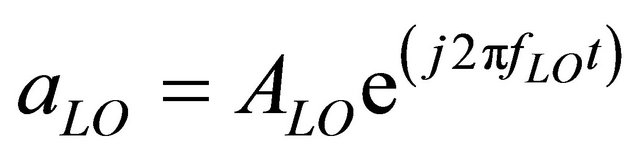
Complex parameters Ak and Bk depend on the S parameters of the RF linear circuit at frequency fLO = fRF. aLO and aRF are the RF and LO input signals, respectively. bk is the transmitted pseudo power wave at ports 3, 4 and 5 of the ring.
We can then write:
 , (2)
, (2)
 . (3)
. (3)
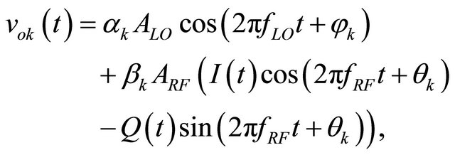
ARF and ALO are the amplitudes of the radiofrequency and local oscillator signals. I and Q represent the inphase and quadrature signals. If the two signals are synchronized, it is assumed that . The three real RF voltages are obtained with the real part of Equation (1):
 (4)
(4)
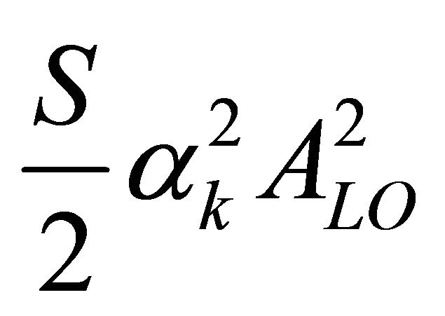
αk and βk are the modulus of Ak and Bk, respectively; φk and θk are their respective arguments. The last term contains the main information to recover.
In practical, the three output demodulator voltages must be measured and then I, Q parameters will be deduced after a calibration procedure. There are several calibration methods like for example the five-port self calibration [14], and the blind calibration [15].
3. Five-Port Correlator Using Microstrip Technology
3.1. Interferometer Circuit
The circular passive five-arm ring is chosen as the interferometric circuit. It is realized using microstrip technology with an epoxy substrate. The ring operates at 2.4 GHz frequency with a bandwidth of 1 GHz. The impedance characteristic of the ring was set to 44.7 Ω. All accesses have an impedance of 50 Ω, which gives symmetry of the device. Figure 2 shows the ring microstrip layout.
The following three figures present the simulation results of the five-arm ring obtained with Agilent Advanced Design System (ADS) environment.
Figure 3 exhibits the curves of the reflection coefficients Sii for i = 1 to 5. All these curves are confounded and shows that the system is well matched since |Sii| < −10 dB for a wide frequency band around 2.4 GHz, and especially at the operating frequency for which Sii = −24.19 dB. Reference [16] indicates that the best magnitudes and phases allowing to have an appropriate estimate of I and Q signals are an equality of  and
and ; and a relative phase of ±120˚ between the three signals.
Vectors representing the three output voltages ,
,  and
and  are rotating according to a Φ rotation. Therefore, there will be a relative phase shift ±Φ between the outputs. However, it is possible to correct this phase shift error by using a calibration procedure.
Figures 4 and 5 show the variations in modulus and phase of S1J parameters depending on the frequency. First note that as well for the magnitude curves as for the phase curves, S12 and S15 (curves in green and red) on the one hand; and S13 and S14 (curves in pink and blue) on the other hand are confounded. As expected, the Five-arm ring operates at 2.4 GHz as a power divider, ensuring an equal distribution of almost half of power (0.503 for S13 or S14, and 0.461 for S12 or S15) to each accesses with a phase shift of +/−120˚ approximately, which will enable us to find both signals I and Q and to obtain the complex envelope of the baseband signal.
3.2. Power Detectors
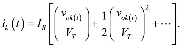
As shown in Figure 1, the Schottky diodes are connected to the interferometer’s outputs. The nonlinear currentvoltage characteristic of these diodes permits their use as power detectors. For small values of voltage across a diode, the current which crosses it presents a low-frequency component due to predominant second-order effects. Equation (5) is the diode Schottky’s law.
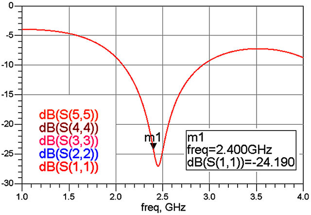
Figure 3. Reflection coefficients Sii versus frequency.

Figure 4. Magnitudes of S1j versus frequency.

Figure 5. Phase differences of S1j versus frequency.
 (5)
(5)
where VT = 26 mV and Is represents the saturation current of the diode (Is = 3 μA for HSMS2850 of Agilent). If the amplitude of the RF input voltage  is lower than VT, Equation (5) can then be approximated as follows:
 (6)
(6)
This approximation is valid for low input power [10], so a linearization technique [12] is used to apply the quadratic law for higher input power. The output port of a RF power detector can be modeled by the diagram of Figure 6, where  is the diode current defined by Equation (6). RV represents the video resistance of the power detector [17], R and C are the components of the low-pass filter.
The voltage  is proportional to the baseband term of
 , which corresponds to the even-order term of Equation (6). The three output voltages
  are:
are:
 (7)
(7)
with .
.
Equation (7) represents the quadratic law of a power detector. By using Equations (4) and (7) and assuming that fLO = fRF, we obtain Equation (8) representing the output voltages  for k = 3 to 5.
 (8)
(8)
with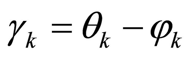 .
.
We see that each voltage is composed of three terms:
•  corresponds to the DC-Offset of the LO self-mixing signal;
•  corresponds to the RF auto mixture. It is the second order inter-modulation term or IM2;
• 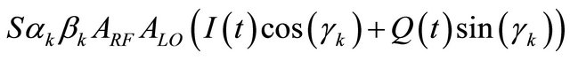 corre- sponds to the mixing signal between LO and RF signals.
The last term is the desired signal I/Q, it carries the information and contains the complex envelope of the RF signal. In the classical receiver, the baseband I/Q signals are directly obtained by two mixings. So, a signal processing must be applied on the three output voltages to reject the dc offset and the even-order terms, and regenerate the I/Q signals.

Figure 6. Equivalent diagram of the output of an RF power detector.
4. Calibration Method
The calibration method of the five-port demodulator is the same as that of the six-port, and the literature related to this subject is numerous [18,19]. When used as a reflectometer, the six-port calibration is both very powerful and complicated because it requires human intervention for the calibration standards (short, open, and matched load).
The calibration procedure consists to determine three complex constants to regenerate the complex envelope from the three output voltages [12]. Some simplifications are applied to the output voltage’s equations so that we can write the expression of signals with the three output voltages and calibration constants.
In Equation (8), the term  can be written as the sum of two terms as follows:
 (9)
(9)
where  and
and  represent the dc and time-variant components, respectively. Equation (8) becomes:
 (10)
(10)
where  is the dc component of the output voltage
 . These components can be estimated by averaging, and eliminated by subtraction. We thus obtain:
 (11)
(11)
 definies the average.
The expressions of the three output voltages after dcoffset cancellation are:
 (12)
(12)
with: 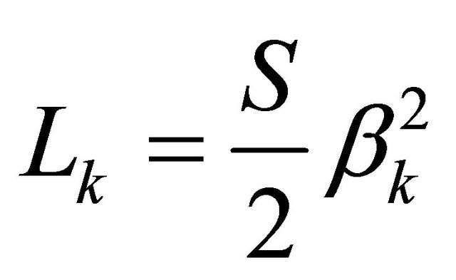 and
and 
The three output voltages  are a linear combination of the three time-variant terms
  and
and  which can be expressed in the following matrix form:
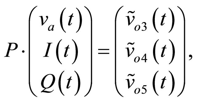 (13)
(13)
where .
.
Assuming the matrix P invertible, it is possible to write:
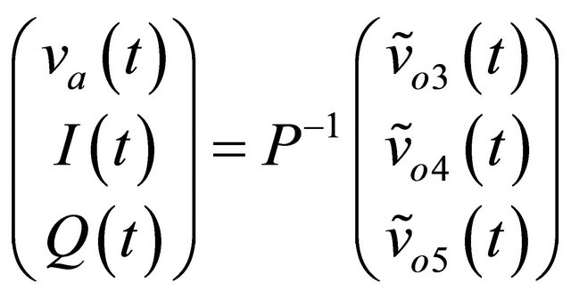 , (14)
where . (15)
From these two relationships, we obtain the following equations:

Equations (16) and (17) define two relations between I (t), Q(t) and the 3 output voltages, and show the six calibration constants  and
and  with k = {3, 4, 5}. Thus, after determination of these constants and measurement of the voltages
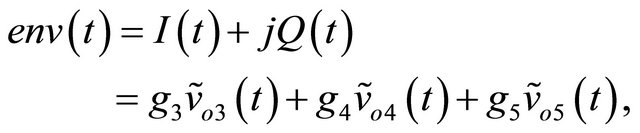
 , it will be possible to regenerate the signals I(t) and Q(t), and obtain the complex envelope of the baseband signal:
 (18)
(18)
with 


g3, g4 and g5 are the three complex calibration constants previously mentioned.
5. Measurement Results
In order to validate this calibration method, measurements were carried out. Two RF generators, Marconi 2031 and HP-4432B, are connected to the input ports 1 and 2 of the five-port correlator, respectively.
A 10 MHz clock synchronizes both generators and a frequency difference Δf = 100 Hz is set between the RF input signals. Let us remind that the five-port calibration is to get the complex calibration constants and thus determine the complex envelope. A simultaneous sampling of the five-port outputs is made by a data acquisition system, the sampling frequency of the acquisition board is set at fs = 10 KHz. The carrier frequency is fixed at 2.4 GHz and the RF generators are set to supply POL = 0 dBm and PRF = −20 dBm of power. We obtain symbols equally distributed along a circle, so the calibration constants generated are reliable. Figure 7 exhibits the result of this calibration procedure.
Measurement results of the three demodulator output voltages are presented in Figure 8.

Figure 8. Magnitudes of v03, v04 and v05 depending on dephasing between RF and LO signals.
The demodulator output voltages are sinusoids resulting from the dephasing between the RF and LO signals. Non-zero phase shift between at least two of the three accesses should be verify to demodulate the signal. Moreover, the redundancy of the five-port correlator architecture allows correcting the interferometer error phases. We note a complementary variation of the three voltages; each one has only one maximum or minimal value for a dephasing between the LO and RF signals ranging from 0 to 360˚. The five-port junction can then be considered as a phase discriminator. Each voltage  is 2π periodic and the three minimal voltage values are separated by multiples of 2π/3. This consideration is used to estimate the directional of arrival of multi-path signals by measuring the phase difference of detected signals [20,21] and also, it is used to estimate the time of arrival by measuring the phase difference over two successive frequencies.
6. Conclusion
In this paper, a new wideband demodulator using a fiveport correlator for channel sounding application has been presented. We focused on three main criteria, which are calibration, phase and demodulation capacity in the whole band. The complex envelope can be evaluated by making power measurements of the five-port wave correlator outputs. In order to accomplish power detection over a larger dynamic, a calibration procedure was used to set aright the five-port correlator imperfections and compensate the phase and amplitude losses in the system. Measurement results were conduced to evaluate the performance of the wideband demodulator, and results obtained with the circuit have shown an excellent agreement between theory, simulations and measurements. In addition of the wideband operating, the five-port correlator has a redundant output allowing it to be more robust against the phase and amplitude unbalance of the local oscillator. Nevertheless, these features will only be exploited if a calibration procedure is applied, which could lead to erroneous results if it is not performed correctly.