1. Introduction
Cadmium Zinc Sulfides (Cd10–xZnxS) have properties in between CdS and ZnS. Addition of Zn to the most widely used CdS buffer layer material enhances the electronic and optical properties of optoelectronics devices. The CdZnS thin film band structure has a larger energy gap than CdS. This makes the material much more attractive for fabrication of solar cells. It has been a widely used as a wide band gap window material in hetrojunction photovoltaic solar cells and photoconductive devices [1,2].
The CdZnS ternary compound is also potentially useful a window material for the fabrication of p-n junction without lattice mismatch in the devices based on materials like CdTe or CuInxCa1–xSe2 [3]. A number of film deposition methods such as spray pyrolysis, sputtering, electro deposition, vacuum evaporation, chemical vapor deposition and chemical bath deposition (CBD), have been used for preparing II-VI compounds [4-7]. Among these, spray pyrolysis is one of the most used methods [8-10]. Compared to other methods, spray pyrolysis has the following advantages: 1) simple and continuous operation; 2) economical; 3) uniform particle size distributions; 4) controllable size; 5) controllable anion and cation concentrations or dopants.
The knowledge of optical constants of materials is frequently of great interest in the design and analysis of materials to be used in optoelectronics. Moreover, optical measurements are extensively used for characterization of composition and quality of the materials. So it is essential to have an insight into the optical properties, which include the optical band gap, reflectivity, absorption coefficient, the dielectric constant and the refractive index as a prerequisite in using the suitable material for device applications.
The aim of this study it is to investigate effect of deposition parameters on the structural and optical properties of Cd10–xZnxS thin films to calculate optical constants such as refractive index and dielectric constant.
2. Experimental Details
Cd10–xZnxS films are prepared onto hot glass substrates by using chemical spray pyrolysis technique The spray solution was prepared by mixing cadmium chloride dehydrate (CdCl2·2.5H2O), zinc chloride (ZnCl2) and thiourea (CS(NH2)2) of molar concentration 0.15 M/L. Depositions were done at 350˚C on cleaned glass substrates.
Two experimental methods were used for thickness measurements; the “Weighting method” and the “Optical interference fringes method”. The Weighting method gives an approximate value for the thickness of the thin films with an error 30%. A digital balance with accuracy of (± 0.1 × 10⁻³ gm) was used for weighting the needed materials and for measured the thickness of the prepared films. He-Ne laser of wavelength 632.8 nm was used for measured the thickness of the films by optical interference fringes method, the thickness of all the prepared films was 280 nm.
The crystallographic structure of the films was analyzed with a (XPERT-PRO) X-ray diffract meter using Cu-Kα radiation with wave length (λ = 1.54060), Current = 30 mA, Voltage = 40 kV, Scanning angle (20˚ - 60˚). The average grain size in the deposition films was obtained from a Debye-Scherrer formula. The optical properties of Cd10-xZnxS films are measured at room temperature by using IR-VIS-UV spectrophotometer at wavelength within the range (300 - 900) nm.
3. Results and Discussions
3.1. X-Ray Patterns
Figure 1 shows the X-ray diffraction pattern of Cd10–xZnxS films for Zn contain between x = 0.1 to x = 0.5 which taken at room temperature. A comparison of the peak position (2θ) values of ASTD XRD spectra data suggests that the as-deposited films have both (zinc blende) cubic and (wurtzite) hexagonal structure with the peak corresponding (111), (200), (220), there are only one sharp and three small peaks present and exhibit polycrystalline structure.
We calculate FWHM theoretical and compared with XRD; it found comparable (as illustrated in Table 1). The average grain size (g) has been obtained from the XRD patterns using Debye-Scherer’s formula [11-13]:
 (1)
(1)
where k =constant taken to be 0.94;
λ = wavelength of X-ray used 1.542 Å;
β = FWHM of the peak;
θ = Bragg’s angle.
It was also observed that the grain size is constant and equal to 5.012 nm, and theoretical was 4.823 nm as Zn content (x value) increase (Table 1).
3.2. Optical Characterization
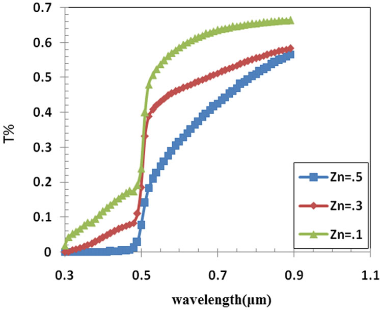
Measured values of transmittance (T), absorbance (A) and reflectance (R) spectra of the films as a function of wavelength (λ) are shown in Figures 2-4 in the UV-Vis spectral range (300 - 900) nm of the films with optimal thickness of 280 nm obtained for each Zn content. It shows a transmittance of 50% - 68% for Zn = 0.1, 50% - 58% for Zn = 0.3, and 18% - 58% for Zn = 0.5; in the (510 - 900) nm, which is high enough for solar cell applications. A shift in the optical absorption edge to low wavelengths (blue shift) is apparent among the transmission curves of the samples when the Zn2+ concentration is increased and Cd2+ concentration decreased in the solution, the films became more transparent in wavelength longer than 500 nm and the curves shifted towards low wavelength. The curve of Zn = 0.3 for the Figures 3 and 4 this means that the optimum condition for the deposition is at Zn = 0.3 which appear in the value of Eg of films.
The relationship between absorption coefficient and optical band gap is expressed to calculate the band gap of the compound by the following relationship:
 (2)
(2)
where A is an energy-independent constant;
Eg is the optical band gap;
m is a constant which determined type of optical transition.

Figure 1. X-ray diffraction (XRD) pattern of (a) Cd9.5Zn0.5S film; (b) Cd9.7Zn0.3S film; (c) Cd9.9Zn0.1S film.

Table 1. The value for all peaks of Cd10–xZnxS film at x = 0.1, 0.3 and 0.5 from X-ray pattern.

Figure 2. The transmission spectrum of Cd10–xZnxS film at x = 0.1, 0.3 and 0.5.

Figure 3. The absorption spectrum of Cd10–xZnxS film at x = 0.1, 0.3 and 0.5.

Figure 4. The reflectance spectrum of Cd10–xZnxS film at x = 0.1, 0.3 and 0.5.
The values of the direct optical band gap (Eg) was determined from the absorbance data by plotting (αhν)2 versus by Figures 5(a)-(c) and then extrapolating the straight line portion to the energy axis α = 0. The band gap energy (Eg) obtained for each Zn contains is different. The band gap of other films was intermediate figures Figures 5(a)-(c) and Table 2. It can also be seen from the figures and Table 2 that Eg for Zn = 0.3 is larger than the other concentrations and this agreement with others [14].
It can be evaluated that the obtained optical band gap values by this method are suitable for many scientific stud1es and technology applications, such as gas sensors, heat mirror, solar cells, transparent electrodes and piezoelectric devices.
 (a)
(a) (b)
(b) (c)
(c)
Figure 5. The energy gap of the Cd10–xZnxS film at x = 0.1, 0.3, 0.5.

Table 2. The optical constant of Cd10–xZnxS film at x = 0.1, 0.3 and 0.5.
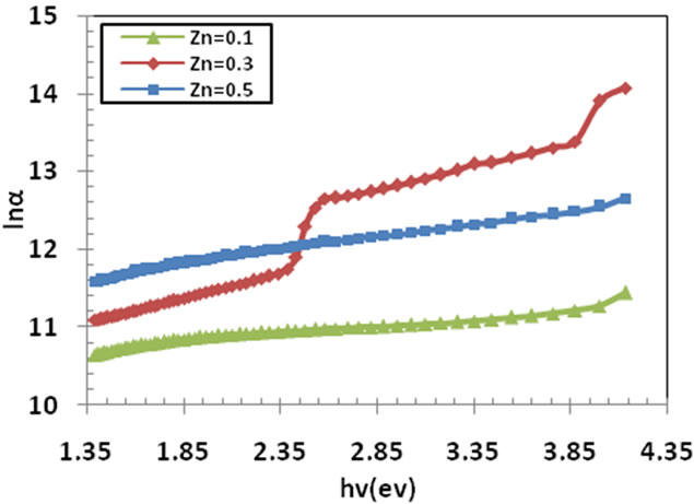
The absorption coefficient near the fundamental absorption edge is exponentially dependence on the incident photon energy and obeys the empirical Urbach relation where (lnα) varies as a function of (hν). The absorption edge in the spectral range of direct optical transitions has exponential shape following the relationship [15,16].
 (3)
(3)
where EU is the Urbach energy which corresponds to width of the band tial; αo is a constant.
Thus a plot of (lnα) vs. (hν) should be linear whose slope gives Urbach energy. The Urbach plots of the films were shown in Figure 6.
Urbach energy was calculated from the reciprocal gradient of the linear portion of these curves and is given in Table 2. EU energy values change inversely with the optical band gap. Some defect during formation of films are formed, these defect produce localized states in the films. Thus the increase in width of the localized states in optical band gap decreases the optical band gap. This means that the thin film becomes more crystalline and this is clear from the Table 2.
Figure 7 Represent the refractive index dependence on the wavelength which calculated by using the following equation [17]:
 (4)
(4)
where R = the reflectance;
k = the extinction coefficient.
The refractive index of the films significantly changes with deposition parameter.
The optical dispersion (Eo and Ed) using Wemple-DiDomenico model which can be easily obtained by plotting of 1/(n2–1) vs. (hv)2. The Ed and Eo values was calculated from the slope (EdEo)–1 and intercept (Eo/Ed) Table 2. The obtained dispersion parameters change with deposition parameters.
The imaginary and real part of dielectric constant of the films was also determined by the following relations [18]:
 (5a)
(5a)
 (5b)
(5b)

Figure 6. The Urbach plots of the Cd10–xZnxS film at x = 0.1, 0.3 and 0.5.

Figure 7. The refractive index (n) versus of wavelength of the Cd10–xZnxS film at x = 0.1, 0.3 and 0.5.
where k = αλ/4π. The imaginary and real part of dielectric constant of the films is respectively shown in Figures 8 and 9. It is seen that both εi & εr decreases with increasing wavelength. The imaginary and real parts follow the same pattern and the value of real part is higher than the imaginary part. The deposition parameters cause important change in imaginary and real parts of the dielectric of the films.
4. Conclusions
• Cd10–xZnxS thin films have been deposited by spray pyrolysis method at 350˚C substrate Temperatures for different deposition parameters. All films were a good adherent and homogeneous.
• The structure of the films was analyzed by X-ray diffraction and the results obtained showed that the film structure is polycrystalline.
• The spray pyrolysis thin films show average transmission values are valid 50% - 68% for Zn = 0.1, 50% - 58% for Zn = 0.3, and 18% - 58% for Zn = 0.5; in the (510 - 900) nm.
• The optical absorption spectra of the films show that the absorption spectra mechanism is due to direct transition.
 (a)
(a) (b)
(b) (c)
(c)
Figure 8. The imaginary of dielectric constant versus of wavelength of the Cd10–xZnxS film at (a) x = 0.1; (b) x = 0.3; (c) x = 0.5.
• The Urbach energies EU were calculated. From the Urbach energy calculation we are found that there are some defect during formation of films but this defect is not effect on its structure, and the film with Zn = 0.3 become more crystalline
• The optical dispersion (Eo & Ed) using Wemple-DiDomenico model were also analyzed. The refractive index (n), the imaginary and the real parts of the dielectric constant of the films were calculated for the films. All of these constants are decreased with wave-length.
• In conclusion, the influence of the deposition parameters on optical properties of Cd10–xZnxS thin films is significant. Because of the optical properties
 (a)
(a) (b)
(b) (c)
(c)
Figure 9. The real of dielectric constant versus of wavelength of the Cd10–xZnxS film at (a) x = 0.1; (b) x = 0.3; (c) x = 0.5.
of the prepared thin films, they can be used as a window material to make a solar cell. The Cd97Zn3S thin film may be assumed as an ideal alternative material to CdS and ZnS since its composition can be simply controlled.
NOTES