Analysis on Micro Complex Shape Via Hole Punching on Low Temperature Co-Fired Ceramics ()
1. Introduction
Once being seen as a promising breakthrough in electronics decades ago, multilayer Low Temperature Co-Fired Ceramics (LTCC) technology went through a downfall after the passing of the millennia due to the process complexity and limited production usage. The upcoming era of industry 4.0 however, is giving a strong push towards a more specified and customized application based electronics. Co-fired ceramics still holds a promising future in electronics. Ceramics is widely used in microelectronics as a monolithic device where the entire support structure, including the conductive, resistive and dielectric materials is sintered at the same instance, creating an independently functioning micro system [1]. The technology is also used in electronic packaging for its high resistance to environmental stress [2].
Casted ceramic sheets are commonly printed with conductive ink on its surface to create electrical paths. The sheets are then stacked in its green state (pre-sintering) where via holes are aligned between the sheets and then filled with conducting material, thus creating an interconnection between the sheets [3]. Quality and alignment of these circular via holes are of utmost importance to achieve a fully functioning system [4]. All via holes are commonly circular due to the ease of the punching alignment and uniformity of the via filling process. Deformed via holes are often regarded as the main cause of functional failure in an integrated device. These via holes are mainly mechanically punched in various sizes depending on the sheet and product. With the advancement of consumer electronics and the ever advancing miniaturization of products, it is only natural there is a need that the size requirements of these micro holes are reduced. The punching process of these holes includes a pneumatic or electric driven punch head that moves in multiple axes and a fixed die. A typical sheet could have as many as 2000 punched holes, all to be aligned with holes or marks on the corresponding sheet. Post-sintering shrinkage is also an important factor in the design and evaluation of the holes [5]. The evaporation of solvents and the combustion of the polymer binder from its green state during sintering process shrink the tape significantly, some deformation naturally occurs [6].
Due to the significant number of connecting holes on a single sheet by reason of its shape, this study analyzes the quality of a complex shaped hole as a substitute for a circular shape. The complex shape which comprises of a combination of circles and rectangles, could pave way to a simpler design of electrical path and less punched hole on a sheet. This study will analyze the quality of a single LTCC sheet without its polymer protection within different parameters such as punch speed, punch depth, sheet thickness, etc. Previous studies conducted on the quality of micro circular holes on LTCC sheets have shown that debris and slugs are a present challenge for mechanically punched vias [7]. Therefore this study also conducts experiments on different punch-die gaps on non-circular holes. The punch process includes a mechanical punch and die fabricated by a self developed machine.
2. Experimental Methodology
2.1. Experimental Setup
Ceramic sheet mainly composed of Aluminum Oxide and some other composite glass ceramics was prepared in its green state with different casted thickness. They were cut into pieces of 15 mm × 65 mm. A multiple axis micro machining equipment is used to create the punch tool and die, embedded along with it a punching stage to carry out the punching process. This equipment, shown in Figure 1 is designed to have a travel repeatability of up to 1 µm on each axis. The two main chambers of the machine, namely the tool fabrication chamber and the punch chamber, lies on the same axis, easing alignment.
The experiment consists of a punch test, in which different parameters of the sheet and punch process are tested, and a gap test, in which various clearance of the tools are tested. In both cases, sheets are punched in their green state and sintered later on.
2.2. Variable Punch Parameters Experiment Design
The complex shape chosen for the experiment is two domes on the end of a rectangle as seen with dimensional values in Figure 2 [8]. Mechanically punched LTCC holes naturally follow die size rather than the punch. Due to the complexity of this particular form, the theoretical gap between the punch tool and die is designed at 10 µm.
The equipment uses Wire Electrical Discharge Machining (WEDG), a method of Electrical Discharge Machining (EDM) technology, to fabricate a micro tool head which in turn machines the die [9]. This tool head will be termed as an Electrode. Due to the complexity of the shape, two dies of the same shape are machined. One for the actual punch process, and the other to create the punch tool by reverse-EDM, a technique where the polarity of the machining is inverted and the die machines the punch tool [10]. In this case, the punch tool and die is made of tungsten carbide. Figure 3 further clear these steps. The male and female sides are machined to a height of 0.2 mm and 0.3 mm respectively.
On top of the different sheet thickness, it should also be proven that punch speed and depth would have various effects on the result of a complex shape via hole. Three different sheet thickness of 250, 300 and 600 µm is tested against 1, 10 and 20 mm/s travel speed and distance of 100%, 110% & 120% of thickness as seen in Table 1. Punch travel is counted from the top layer of the sheet.
2.3. Variable Gap Experiment Design and Parameters
S. H. Rhim et al. stated that massive burr occurs as tool tolerance increased in double layer green sheet with PET Mylar on circular via holes [11]. In order to prove that this statement still applies on non-circular via holes, further experiments are conducted on different gap sizes. For this test, the shape is chosen to be a 100 µm × 120 µm rectangle. To achieve this, micro electrode made of tungsten carbide is directly machined into the required punch tool shape with the tip having a smaller size than the body with WEDG. The tip is then used to construct the die. The die used in the experiment is a copper sheet of 0.3 mm thickness. EDM machining process naturally creates a gap between the two parts, which is ideally 10 µm. The tip is then cut-off and the rectangular electrode is used to punch the workpiece [12]. Various electrodes prepared with different tip dimensions enable the creation of different tool clearance, the smaller the tip size the smaller the gap. The experiment uses three different tip offsets, the first same size as the body, 5 and 10 µm smaller as seen in Figure 4. All punch tests are done on the same travel speed of 20 mm/s.
![]()
Figure 2. Form and dimension of complex shape punch tool and die.
![]()
Figure 3. Tool fabrication and punching process of complex shape via hole.
![]()
Figure 4. Different stepped tungsten carbide electrode tip offset used to fabricate different punching gaps.
![]()
Table 1. Punching parameters of complex shape via hole (in µm).
2.4. Measurement
All test results are observed with an Olympus STM6 measuring microscope pre and post sintering. Formation of warpage is analyzed through a Scanning Electron Microscope (SEM). To improve scanning results, the workpieces are coated through vapor deposition of gold (Au). The resolution imitated of the coating is 0.1 µm hence negligible. The co-firing process starts with burning out of the solvents at 300˚C for 50 minutes and then sintering at 900˚C [13]. The complete spectrum can be seen on Graph 1.
3. Results and Discussion
Results of the experiments conducted was used as base to observe and investigate tool fabrication and punched hole quality. Figure 5, a microscope image of the double circle complex shape, calculates to a gap of 9.022 µm in the vertical direction, an offset of about 1 µm from its designed value. Measurement is also taken on the centre distance of two circles and in this case shows an adequate precision for the test. Certain level of roughness is detected on the corners of the punch tool due to the nature of the reverse-EDM but can be omitted due to its minute extent.
Electrode was successfully shaped into a rectangle with each corner at 90˚ ± 1˚. Figure 6 shows the electrode after the first and second sides cut off. Locating the center of the electrode was of utmost importance as to get an exact sizing of the shape, as the machine spindle core does not necessary correlate to the electrode center point. Some challenges were met during the tool making of the gap test, namely to fabricate a micro tip of 10 µm and 5 µm with the machine’s accuracy of 1 µm and the feeding rate of EDM. Spark gap between the electrode and workpiece in EDM is an unavoidable phenomenon that results in an inevitable error.
That being said, the tips were produced and Figure 7 shows the difference of the straight tip and the smaller tip of 10 µm, where the height (H) of the straight electrode rectangle was measured at 118.927 µm. Whereas the total difference of the inner tip and main body of the stepped electrode stands at 18.599 µm (L2 - L1), each side with a dimension and accuracy of 10 µm ± 2 µm.
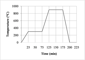
Graph 1. Experiment sintering temperature and duration.
![]() (a)
(a) ![]() (b)
(b)
Figure 5. Fabricated (a) punch die and (b) punch head measurements.
![]()
Figure 6. Corner angle value of rectangular electrode.
![]() (a)
(a) ![]() (b)
(b)
Figure 7. Tungsten carbide electrode with different tip offsets: (a) side view of straight no offset tip and (b) side view of 10 µm offset tip.
Table 2 shows the dimensions of the rectangular punch tool and die height and length with the average of 5 measurement takings. It can be deduced that the tools were successfully machined to its acceptable dimensional requirements. Punch tool with 10 µm offset resulted in a die size about 3 µm larger than the electrode punch head.
Images on Figure 8 and Figure 9 show the quality of the electrode punch and copper die. Some circular indentation can be seen on the female die that is not seen on the male punch tip. This is assumed to be due to the uneveness of the EDM rate. Workpiece punch results will take into account whether or not these shapes are translated into the ceramic sheets.
![]()
Figure 8. SEM image of copper rectangular die mold with no offset.
![]()
Figure 9. SEM image of electrode punch mold no offset tip.
![]()
Table 2. Average measured dimensions of rectangular punch tool and die height and length.
3.1. Variable Punch Parameters Experiment Results
Samples gathered were measured in the concentric center distances of the two circles (L) and the height of the rectangle (H) taken from its top view. An average of 3 measurement of each sample was calculated. Table 3 shows the full outcome group in terms of different speed on the main row and different sheet thickness on the main columns. Taken the target size of L to be 460 µm, Graph 2 explicitly shows that the 600 µm sheet thickness has a significant offset the required line. It averages an offset of 8.356 µm from ideal. It is also true that compared to the other two thickness, it is has the poorest result. It is also evident that deeper punch distance has an effect towards the result as the graph shows a downward trend on almost every line. The same manifests in the H dimension, where different depths brings the size closer to the desired size. On the contrary, travel speed did not have too large of an effect. Although there are some improvements at the accelerated punch speed, but they are overall minimal. This is assumed due to the nature of pre-sintered LTCC tapes that are flexible hence the shearing force initiates fracture at a much lower requirement.
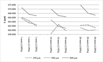
Graph 2. Comparison of pre-sintered via circle distance in terms of punch speed and sheet thickness.
![]()
Table 3. Pre-sintered complex shape via hole punched result measurement (in µm).
Representation shown on Figure 10 is taken from 110% at 10 mm/s for different sheet thickness. It is rather noticeable that there are darkened shades on the edges of the 600 µm sheet, which means the hole is on an angled slope. Similar instances are found throughout samples from this thickness, making it questionable for further usage. The limited to none existing shades at the 250 µm and 300 µm samples indicates that the samples are rather straight and satisfactory for further handling. Both these thicknesses show promising results in terms of average calculated size and hole features.
Results seen from SEM images also confirms that the complex shape of the two lesser thicknesses comply with quality required for via filling, i.e. minimal burrs on the sides and no displacement of ceramic particles. The picture shown in Figure 11(a) explains from a top view, a clean cut is produced and there are minimal rough corners around the rectangular path. Figure 11(b) shows the innate character of a punched green state sheet where the inner walls exhibit pre-bonded ceramics. The thicker thickness of 600 µm had poorer quality across the corners and a less smooth cut. Some particles measured were up to 70 µm in size and may have an adverse effect on the electrical properties after via filling. These phenomena can be seen across samples of this particular thickness with the example given in Figure 12. It also demonstrates that particle build up starts not just from the corners at the top but also from along the inner body walls, most likely due to uneven mixing of slurry during sheet casting on PET sheet. Standard procedures of via filling allow some degree of surface and corner irregularity because they are likely to disappear or flatten during the sintering process. That being said, the magnitude of these proportions is typically not accepted.
![]() (a)
(a) ![]() (b)
(b) ![]() (c)
(c)
Figure 10. Measured dimension of (a) 250 µm, (b) 300 µm and (c) 600 µm pre-sintered holes on its top view.
![]() (a)
(a) ![]() (b)
(b)
Figure 11. (a) Top and (b) tilted SEM view of 300 µm sheet punched at 120% of thickness and 20 mm/s.
![]()
Figure 12. SEM image of a 600 µm LTCC sheet punched at 20 mm/s and 120% of thickness punch depth.
3.2. Variable Gap Experiment Results
Three sets of samples were taken for each gap clearance tests. Male punch tool with no offset would have a gap of 10 ± 2 µm, 5 µm offset to have a gap of 5 ± 2 µm, and 10 µm offset to be 0 ± 2 µm. Results of the experiments can be seen in Table 4. Results were calculated based on an average of 5 measurements on the same sample. Agreeing to earlier experiments that hole sizes correspond more towards female die size, we take the female die size as the target height and length. The outcome unexpectedly shows that the different gaps do not have a major impact on the overall hole size.
Displacement averages at 2.700 µm across the different offsets, showing promising results. Figure 13 compares the three different gaps corner and surface smoothness: It is noticeable that the two smaller gaps does have an impact on the quality of the corners. The largest gap creates a rather slanted corner whereas the smaller has a sharper edge. That being said, these are small enough to be negligible. It can be assumed that the initial gap created by the tip with no offset, which resulted in a gap distance purely of the EDM feed, was already an adequate gap for LTCC process usage, and a smaller gap would only reinforce it.
3.3. Post-Sintering
SEM image on Figure 14 shows a post co-fired complex hole. This substrate was punched at 10 mm/s at 110% of its thickness. No apparent burrs are seen on any of the corners and surfaces of the holes as is typical in sintered LTCC. Sintered substrates also had good mechanical character and the complex shape was not deformed in any way. The fragile stages of the substrate when all its binders and plasticizers evaporate and where it loses a portion of its volume did not destruct the complex shape from its initial profile. Similarly, the densification of the tape looks to be uniform and does not injure the original shape.
On average, the holes shrink on its length slightly more than on its height. Table 5 shows that taken the average, L shrinks 13.18% and H shrinks 10.41%. This does cause a slight misshape of the two circles and rectangle, but would also be apparent on normal post-sintered circular via holes at a similar rate.
![]() (a)
(a) ![]() (b)
(b) ![]() (c)
(c)
Figure 13. Microscope measurements of rectangular via hole on a 300 µm LTCC sheet with different punching clearance of (a) 10 µm, (b) 5 µm and (c) <2 µm respectively.
![]()
Figure 14. Entrance side of sintered complex via hole on a single layer 300 µm LTCC sheet.
![]()
Table 4. Variable gap punch on a 300 µm LTCC sheet measurement result (in µm).
![]()
Table 5. Sintered LTCC complex hole dimension measurement and shrinkage rate.
4. Conclusion
In this paper a more complex shape is chosen as a substitute for a circular shape via hole in the LTCC processing. Punching experiments done with different parameters bore different outcomes. It can be concluded that punching speed is less of a factor than the travel distance of the punch as seen in Graph [1]. Promising results are found on complex shape holes on sheets with a thickness of 250 µm and 300 µm at both pre and post sintering stages. The thicker 600 µm sheet however exhibited poorer result with larger offset and drafted surfaces. The good condition of these sheets post-sintering gives a strong argument in the actual usage of more complex shape via holes. Different gap sizes conducted on rectangular shape demonstrate that a gap of 10 µm is sufficient for punching LTCC sheets as is commonly used in the industry. Any value below the offset of 10 µm does not give a significant improvement in the measured size, albeit fabricating a slightly sharper edge.