The Effect of Light on the CVC of Strained p-n-Junction in a Strong Microwave Field ()
Received 9 October 2015; accepted 28 December 2015; published 31 December 2015

1. Introduction
Research of the effects associated with the heating of the carriers reveal new properties of semiconductor materials and devices, and the physical processes occurring in them that are difficult or even impossible to study in equilibrium conditions of the carriers and the lattice. Interest in the study of hot carriers is caused mainly by the following circumstances. First, the heating of the carriers leads to a change in their energy distribution. This is evident in the well-known kinetic effects, and leads to the emergence of new phenomena unique to the state of the hot carrier’s gas. Secondly, the presence of preheated charge carriers leads to a number of features in the behaviour of semiconductors, which are inhomogeneous in their structure, particularly having p-n, n+-n-junc- tions and others (change of voltage-current characteristics, amplification of current, and the occurrence of additional heat, thermal and photo-thermal emf’s in certain conditions and others). Thirdly, the effects caused by the heating of the carriers, are increasingly used in practical application. On the basis of various kinds of instabilities of current accompanied by the heating effect, radio-electronic devices were created, many of whom work in the microwave frequencies.
In recent years, much attention is paid worldwide to research and development of electromechanical transducers and sensors based on homogeneous semiconductors and semiconductor devices. Small and sensitive sensors and sound detectors, working in a wide frequency band, are needed in many areas of technology.
Connection of the mechanical and electrical properties of semiconductors is determined by two major phenomena: the piezoelectric and deformation effects. Piezoelectric effect occurs in the crystals, which are not an observer inversion center. The deformation effect is due to the interaction of electrons with the crystal lattice, which is available in all semiconductors. The physical cause deformation effects are the shift of the energy levels of the semiconductor under the influence of the deformation and the associated change in the spectrum of the current carriers―electrons and holes, depending on the strain.
Changing the current in semiconductor devices under pressure was first observed in 1951, when p-n-transi- tions to Germany were subjected to uniform compression [1] . Since then, there were many works that investigate physical phenomena in semiconductor devices under pressure, and the possibility of their technical use as electromechanical transducers [2] . [3] analyzed the decay of nickel precipitates in silicon under the influence of a comprehensive hydrostatic pressure. [4] examined the effect of hydrostatic hydrostatic compression (HCV) in the decay rate of a solid solution of Si
at different temperatures.
[5] studied the change characteristics of the photovoltaic silicon p-n-junctions in a microwave field. It is shown that the barrier height of p-n-junction in a strong microwave field, reducing the barrier illuminated p-n-junction, is proportional to the height of the initial barrier, if the latter is reduced by direct displacement. In [6] the current-voltage characteristic (CVC) of strained p-n-junction in a microwave field is investigated and it has been showed that the deformation increases the current generated in the p-n-junction.
From the foregoing, it follows that the calculation of the current characteristics of p-n junctions in a microwave field does not include the impact of a simultaneous deformation and light on the current-voltage characteristics of p-n-junction in a strong microwave field.
The purpose of this work is to study the effect of light on the CVC of strained p-n-junction in a strong microwave field.
2. Theoretical Calculations of the Effect of Light on the CVC of Strained p-n-Junction in a Strong Microwave Field
In the first look at the CVC of strained p-n-junction with the low power of the microwave when there is no heating of the electrons and holes (Te = Th = T) in the absence of the effect of light and disturbance potential barrier height (Ic = 0 (Is―light current), UB = 0). Under these conditions, for the CVC of p-n-junction we have the following form:
 (1)
(1)
where: ;
; ―saturation currents for electrons and holes; j0 the height of the potential barrier in the absence of an electromagnetic wave;
 ; U―a voltage across the diode;
 ―AC voltage of the
incident wave created by the barrier diode; T is the temperature of the lattice; k―Boltzmann constant; Te, and Th― temperature electrons and holes; Eb―electric field of the wave; e is the charge of the electron.
For silicon p-n-junctions saturation currents is as follows:
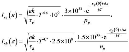 (2)
(2)
where: ―permanent deformation
 ―the band gap of silicon; nn and pp― the concentration of majority carriers; τe and τz―lifetimes for electrons and holes. Then CVC p-n-junction becomes:
 (3)
(3)
From this we can derive an expression for the coefficient of imperfection:
 (4)
(4)
For the CVC strain p-n-junction with the low power of the microwave when there is a perturbation potential barrier height (Ic = 0, e ≠ 0 (e―deformation); Te = Th = T; UB ≠ 0) of formula (1) can be obtained:
 (5)
(5)
Hence, under these conditions, to m, we have:
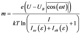 (6)
(6)
Again at low powers the microwave if there is a disturbance potential barrier height and the influence of light (Iс = 0, e ≠ 0; Te = Th = T; UB ≠ 0). Again at low powers the microwave if there is a disturbance potential barrier height and the influence of light:
 (7)
(7)
From  (8)
(8)
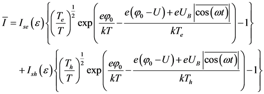
At high power microwave energy, when electrons and holes are hot and happening outrage potential barrier height without lighting (Iф = 0, e ≠ 0; ; UB ≠ 0). CVC strain for the p-n-junction can be obtained ratio:
![]() (9)
(9)
If![]() , the major share of investing Th, then m is determined from the second member (9):
, the major share of investing Th, then m is determined from the second member (9):
![]() (10)
(10)
If ![]() m is determined from the second member (9):
m is determined from the second member (9):
![]() (11)
(11)
For the CVC of strained p-n-junction at high power microwave energy, when electrons and holes are warmed and illuminated p-n-junction, and the place, the height of the potential barrier (e ≠ 0;![]() ; Iф ≠ 0, UB ≠ 0) can obtain the following formula:
; Iф ≠ 0, UB ≠ 0) can obtain the following formula:
![]() (12)
(12)
If ![]() m is determined from the second and third members (12):
m is determined from the second and third members (12):
![]() (13)
(13)
And if ![]() it is determined m the first and third members (12):
it is determined m the first and third members (12):
![]() (14)
(14)
From the above analysis it is possible to build a p-n-junction current-voltage characteristics under different conditions (Figure 1).
![]()
Figure 1. CVC p-n-junction, provided: 1―without deformation, without the microwave field without lighting; 2―in the deformation, the height of the potential barrier (at low powers the microwave) and without light; 3―during deformation, the height of the potential barrier (at low microwave power of the wave) and light; 4―without deformation at high power microwave energy and without lighting; 5―in the deformation at high power microwave energy and without illumination; 6― in the deformation at high power microwave energy and lighting.
3. Conclusion
Based on these studies, the following conclusions can be stated: if light, deformation and microwave field act to the p-n-junction, the deformation and the microwave field increase the current through the p-n-junction, and the light decreases it. The mechanism of this phenomenon is explained by the fact that under heating of the charge carriers by microwave field the recombination current arises, and under the action of light the generation current arises which are directed oppositely. And under the influence of the deformation the band gap of the semiconductor will be changed. As a result, the energy of the electrons and holes will increase, respectively; recombination current also will increase, whose direction corresponds to the direction of the major charge carriers.