Detailed Micro Raman Spectroscopy Analysis of Doped Silicon Thin Film Layers and Its Feasibility for Heterojunction Silicon Wafer Solar Cells ()
1. Introduction
Heterojunction with intrinsic thin layer (HIT) solar cells has proven to be a suitable candidate for cost reduction in industrial high efficiency crystalline silicon (c-Si) wafer solar cells, due to the significantly lower thermal budget requirements [1], allowing the usage of much thinner wafers (<100 µm). In fact, Panasonic has recently attained record conversion efficiencies of 24.7% [2] for a wafer size of 101.8 cm2 and 98 µm thick. To achieve higher conversion efficiency of heterojunction silicon wafer solar cells, the optimisation of the heavily doped thin-film emitter and back surface field (BSF) layers are important [3].
Moreover, it was found through a series of H2 effusion experiments [4], that the addition of doped silicon thin films may lower the passivation quality due to Fermi energy dependent Si-H bond rupture in the a-Si:H films, for either type of doping. This can result in silicon dangling bonds creation, counteracting intentional doping of the a-Si:H matrix and reduce the field effect passivation. Increasing doping concentration is also associated with increased defect densities, which results in Fermi level pinning, and linked to enhanced recombination at the a-Si:H/c-Si interface [5]. Hence, the optimisation of the doped silicon thin film layers is essential to its application in heterojunction silicon wafer solar cells. Despite the challenges, the successful application of doped microcrystalline silicon thin film to heterojunction silicon wafer solar cells has been demonstrated [6-11]. Various characterisation techniques are available for silicon thin film layers. In this paper, we highlight how the usage of μ-Raman spectroscopy has been instrumental in our optimisation process to achieve device quality doped silicon thin films, while not degrading the underlying intrinsic buffer layer and its c-Si/a-Si:H(i) interface quality.
We present recent research work that complements the well-established published works on a-Si, and µc-Si:H related thin films [12-17]. Through the μ-Raman analysis of doped silicon thin films with different microstructures, qualitative and quantitative information on the bond angle deviation, nature of film stress, correlation length and degree of short range order can be deduced. These in-house developed doped silicon thin films are further evaluated to accomplish both (i) efficient field effect passivation and (ii) interface defect density reduction evident from measured injection dependent effective lifetime curves of symmetrically passivated heterojunction lifetime samples [p+/i/c-Si(n)/i/p+], as well as heterojunction solar cell structure [p+/i/c-Si(n)/i/n+]. In particular, our lifetime structure with doped layers shows improvement across all injection levels of interest. From the extracted minority carrier lifetime of 2.4 ms at an injection level of 1015 cm−3 , we infer an excellent surface recombination velocity of Seff ~ 6 cm/s if we assume a bulk lifetime of τbulk = ∞ for the float zone wafer utilised in this work. This is comparable to passivation by the best SiNx or AlOx passivation schemes available elsewhere. Further simulation studies are also conducted to predict the influence of interface defect density on the effective carrier lifetime curves, and consequently on the heterojunction silicon wafer solar cell performance.
2. Experimental Details
Our in-house developed p-doped emitter and n-doped back surface field layers were deposited using a conventional 13.56-MHz parallel-plate PECVD reactor (MVSystems Inc., Cluster-tool, Colorado, USA) at different H2/SiH4 gas flow ratios, doping gas flows, and film thickness, while maintaining the RF power density, deposition pressures, and substrate temperatures as discussed in [18].
Firstly, to investigate the impact of doping concentration on the film, the doping gas flow (B2H6 and PH3) has been varied from 1 sccm to 4 sccm, while maintaining the film thickness at ~40 nm as seen in Tables 1 and 2 below. Secondly, we investigate the impact of increasing thickness for one of the chosen deposition conditions on the μ-Raman results. Thirdly, given that the heterojunction silicon wafer solar cell typically consists of a symmetrical thin intrinsic a-Si:H layer for passivation [19-22] before the deposition of the thin doped layers, we also investigate the impact of substrate type on doped silicon thin film growth (i.e.: intrinsic a-Si:H and glass substrates). The doped silicon thin film on an a-Si:H substrate is prepared by depositing a thin intrinsic a-Si:H layer of ~5 nm on a microscopic glass substrate before depositing the doped layers of ~10 nm with different
Table 1. Overview of process parameters for p-doped silicon thin films.
Table 2. Overview of process parameters for n-doped silicon thin films.
hydrogen dilution ratios R = H2/SiH4. In all depositions, the RF power density, deposition pressure p, and substrate temperature T were maintained at 0.07 W/cm2, 1.9 Torr, and 180˚C respectively.
Finally, based on the analysis, we select one of the optimum deposition condition, and investigate the quality of the doped silicon thin film layers in heterojunction carrier lifetime structures, and device structures on double-sided polished planar low-resistivity (2.6 - 3.1 Ωcm) n-type Fz Si wafers with (100) orientation.
The μ-Raman measurements were performed using the Renishaw inVia Reflex Raman microscope, and utilizes a backscattering geometry with a 514 nm laser line, obtained from an Argon-ion laser. The power of the incident light is 25 mW, and a 50× objective lens giving a laser spot diameter of 5 μm. During each measurement, the exposure time was chosen as 10 s, an accumulation of ten times to improve the signal to background noise ratio, and only 10% of the laser power was utilized to prevent crystallization of the sample. No input polarisation was utilized. All measurements were performed at room temperature. For every sample, 5 separate locations were measured to check for consistency.
In addition, the thickness and sheet resistance of the films was obtained by stylus profilometry (Dektak, Bruker Corporation) and four-point-probe setup (Cresbox, Napson Corporation) respectively. The injection dependent effective lifetime curves are measured using a contactless flash-based photoconductance decay tester (WCT-120, Sinton Consulting) operated in both transient and quasi steady state mode [23].
3. Results and Discussion
3.1. Impact of Doping Gas Flow
Firstly, the impact of the doping gas flow on the μ-Raman spectra of doped silicon thin film on glass is investtigated. Figure 1 shows a decomposing of the μ-Raman spectra for one of our typical microcrystalline silicon thin film into its components for amorphous Si phase, defective Si phase, and crystalline Si phase at 480, 510 and 520 cm−1 respectively [24] and the crystallinity of the thin film χc can be deduced based on the intensity ratio of the crystalline components to that of total integrated intensity as per Equation (1) [25].
 (1)
(1)
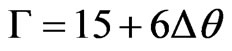
Based on both theoretical investigations as well as experimental evidence, the relationship between root mean square (rms) bond angle dispersion Δθ and the full width half maximum Г of the amorphous silicon transverse optical (TO) Raman peak can be expressed according to
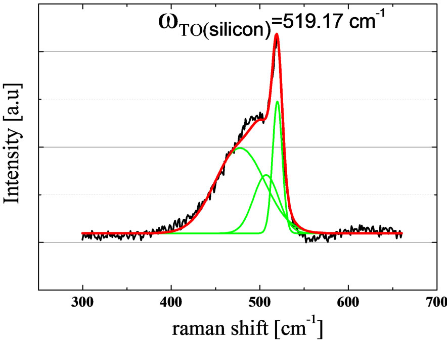
Figure 1. Raman spectra of sample P3. The black, green and red lines correspond to the measured Raman spectra, the Gaussian fits for the three silicon phases, and the resulting fit respectively. The peak position of the crystalline TO spectral band ωTO(silicon) corresponds to 519.17 cm−1 for this sample.
Beeman-Tsu et al. [26] in Equation (2)
 (2)
(2)
It is appropriate to highlight that the bond angle of stress-free crystalline silicon is 109.5˚ and Δθ = 0˚.
By comparing the µ-Raman spectrum in Figure 1 to a typical pure a-Si sample, the appearance of the crystalline components in the µ-Raman spectrum indicates that the chosen deposition conditions facilitate the growth of silicon crystallites. By deconvolution of the µ-Raman spectra for this particular doped sample, the amorphous silicon TO spectral band (ωTO(a-Si)) peak position frequency, its linewidth (Г), and film crystallinity (χc) are extracted as 477.5 cm−1, 65.9 cm−1 and 39% respectively. The same information is extracted from all samples in this work.
Figures 2 and 3 show a plot of film crystallinity and conductivity as a function of the doping gas flow. As the doping gas flow is gradually increased from 1.0 sccm to 4 sccm, the conductivity improves up to a limit before degradation occurs, while the film crystallinity reduces generally. The addition of dopants has reduced the film crystallinity, leading to an increasingly amorphous state. This implies a very narrow doping process window to get both high conductivity for the doped silicon thin film and minimum changes to the doped film microstructure, consistent with reports by Street [27] on the low doping efficiency in the range of 10−3 to 10−1. Fedders et al. [28] has attributed this low doping efficiency for the case of boron doping to the fact that most boron atoms are incorporated into threefold coordinated sites and is non-doping in this configuration, which is in line with Mott’s 8-N rule of bonding [29] for amorphous semiconductors.
Our extracted film crystallinity and conductivity as a function of doping flow provides an alternative support to the above claims, and highlights the importance of doping flow optimisation amid other deposition parameters. The optimum doping gas flow for the p-doped silicon thin film and n-doped silicon thin film was found to be B2H6 = 2.2 sccm and PH3 = 2 sccm respectively. At such doping flow, a sufficiently high conductivity for the p-doped and n-doped thin film is achievable at 1.8 S/cm and 16 S/cm respectively. Increasing doping flow beyond the optimum point will only increase non-electrically active dopant atoms, which can act as recombination centers for minority carriers in a solar cell device, hence reducing the current collection efficiency.
Figures 4 and 5 show a plot of the deconvoluted amorphous silicon TO Raman peak position frequency (ωTO(a-Si)) and crystalline silicon TO Raman peak position frequency (ωTO(silicon)) for different diborane (B2H6) doping gas flow. Increasing the B2H6 gas flow shifts the a-Si TO peak position frequency from 476 cm−1 and approaches 480 cm−1. On the contrary, the crystalline TO
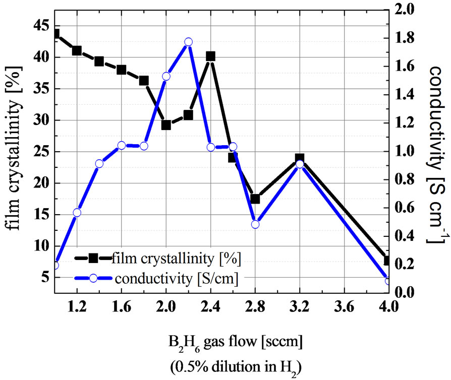
Figure 2. Comparison of film crystallinity % and conductivity for p-doped silicon thin film with different diborane (B2H6) gas flow.
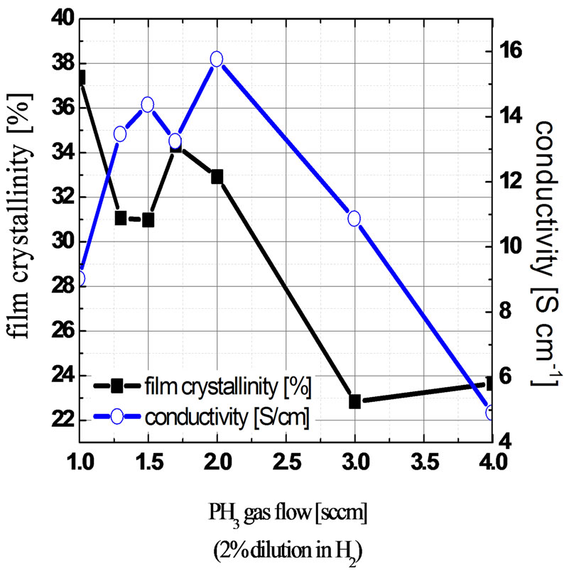
Figure 3. Comparison of film crystallinity % and conductivity for n-doped silicon thin film with different phosphine (PH3) gas flow.
peak position frequency remained at 519.17 cm−1 for B2H6 doping gas flow up to 1.6 sccm, before decreasing for further increase in doping gas flow. It has been reported through 216-atom modelling of a-Si [30] that the correlation (bond) length is related to the vibrational mode localization state at different frequencies. At low frequencies below 400 cm−1, the vibrational modes are fully delocalized, localization increases above 400 cm−1 and for ω ≥ 520 cm−1, the modes are strongly localized. In perspective, since our results shows an increasing ωTO(a-Si) with doping gas flow, it suggests that the vibrational modes are increasingly being localized as well, with the reduction in the bond length, which is reasonable considering the increased quantity of incorporated dopant atoms in the same thickness and volume of the
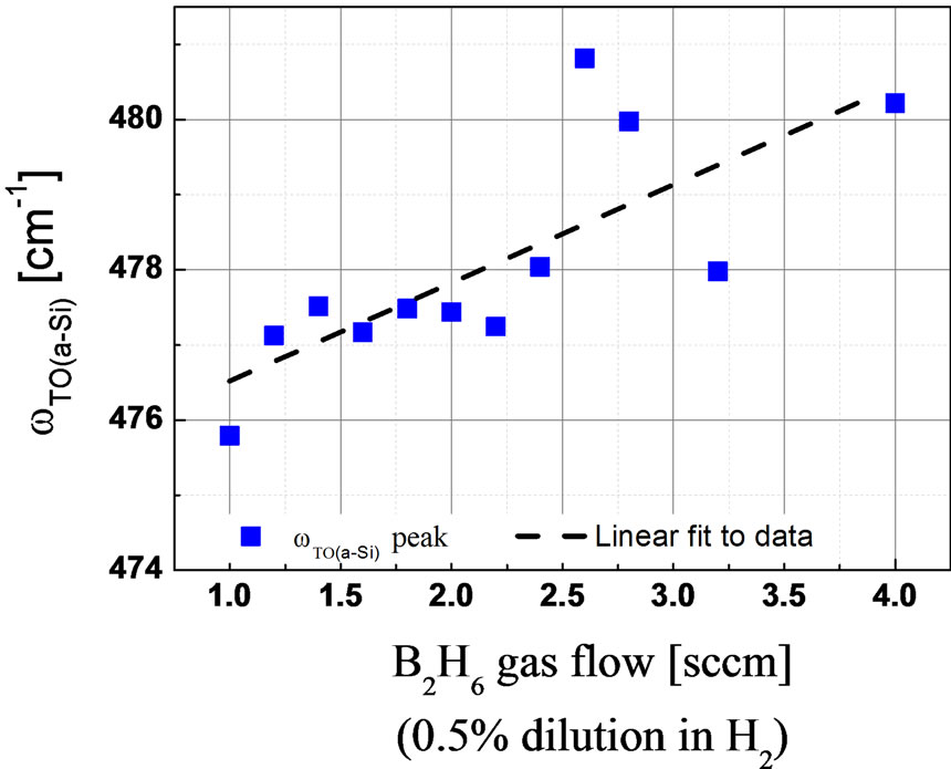
Figure 4. Impact of the diborane (B2H6) gas flow on the amorphous TO Raman peak ωTO(a-Si:H). The line serves as a guide to the eye.
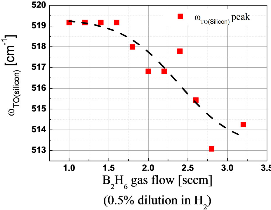
Figure 5. Impact of the diborane (B2H6) gas flow on the crystalline TO Raman peak ωTO(silicon) as extracted from the peak fitting of respective Raman spectra. The line serves as a guide to the eye.
deposited silicon thin film. Furthermore, as compared to a stress free frequency of ω0 = 520.91 cm−1 in crystalline silicon, it is generally agreed that a Raman shift frequency larger than the stress free frequency indicates compressive stress in the sample, while a Raman shift frequency smaller than the stress-free one indicates tensile stress [31-33]. Judging from our results, it is clear that increasing the doping concentrations leads to increased tensile stress in the doped silicon thin film. Using the stress equation from Anastassakis [34] developed for a-Si:H(i) as an approximation, the stress can be deduced according to Equation (3)
 (3)
(3)
where σ is the in-plane stress and  where ω0 is the optical phonon wave number of the stress free single crystal and ωs is the wave number of the stressed sample. In particular, our p-doped samples exhibit tensile stress ranging from 432 MPa at low doping to 1.6 GPa at high doping levels, which can be significant considering the typical thin layers to act as either the emitter or the back surface field layers. Similar discussion applies for the phosphorous-doped silicon thin film layers as observed in Figure 6. The high tensile stress can potentially degrade the underlying intrinsic buffer layer which is responsible for the surface passivation of the c-Si substrate. We highlight later in Section 3.5 the influence of the surface passivation quality on the simulated effective lifetime curves and the corresponding HIT cell efficiency.
3.2. Film Thickness Dependency
Secondly, with the chosen deposition conditions as per sample P6 with a B2H6 doping gas flow of 2.0 sccm, several p-doped silicon thin film samples were deposited on microscopic glass substrates with varying thickness from 20 nm up till 100 nm in 20 nm steps. Figure 7 shows the µ-Raman spectra of these samples, while Figure 8 shows the corresponding plot of film crystallinity and conductivity. It is clear from Figures 7 and 8 that as the film thickness increase from 20 nm to 100 nm, the film evolves from a purely amorphous phase into a microcrystalline phase in which film crystallinity χc increases from 1% to 42%. This change correlates well with an increase in conductivity from 0.06 to 4.8 S/cm.
Similarly, by deconvoluting the Raman spectra into its amorphous and crystalline silicon components, useful information can be determined to explain the observation in Figures 7 and 8. Figure 9 shows a plot of the bond angle disorder extracted from the linewidth (Г) of the amorphous silicon peak position frequency ωTO(a-Si) using Equation (2). The bond angle disorder is observed to
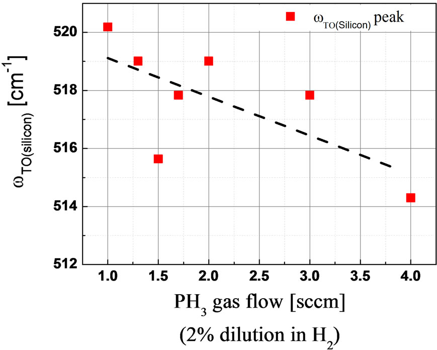
Figure 6. Impact of the phosphine (PH3) gas flow on the crystalline TO Raman peak ωTO(silicon) as extracted from the peak fitting of respective Raman spectra. The line serves as a guide to the eye.
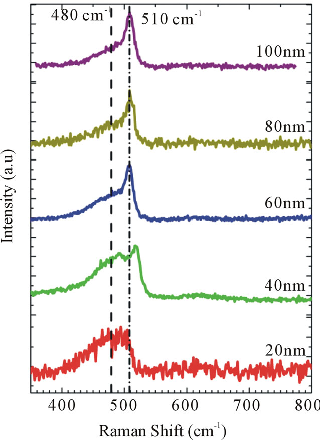
Figure 7. Raman spectra of five p-doped Si films of different thickness. Deposition conditions: pressure 1.9 Torr, substrate temp 180˚C, dilution ratio R = 32, diborane (B2H6) gas flow 2.0 sccm.
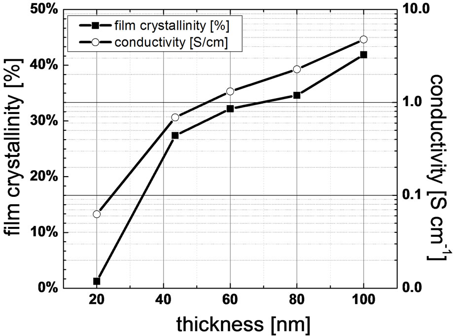
Figure 8. Impact of doped film thickness on film crystallinity and conductivity.
decrease with growing thickness, from Δθ = 110 at 20 nm to Δθ = 80 at 100 nm. Furthermore, as seen in Figure 10, the amorphous silicon peak position frequency increases with increasing thickness from 474 cm−1 at 20 nm to 483 cm−1 at 100 nm. Concurrently, Figure 11 shows that the crystalline silicon peak position frequency decreases with increasing thickness, from ~518 cm−1 at 40 nm and saturates at ~508 cm−1 at 60 nm, 80 nm and 100 nm. From this data, it is indicative of a structural relaxation with increasing doped film thickness, as the film evolves from amorphous into microcrystalline state with increasing film crystallinity, reduced bond angle dispersion Δθ and reduced bond length, similar to other reports [35-40]. However, an increased tensile stress is observed with thicker doped film which is undesired. It is appropriate to
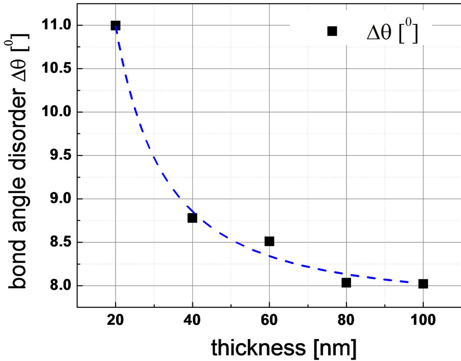
Figure 9. Variation of bond angle disorder Δθ on increasing p-doped silicon thin film thickness on glass substrate. The line serves as a guide to the eye.
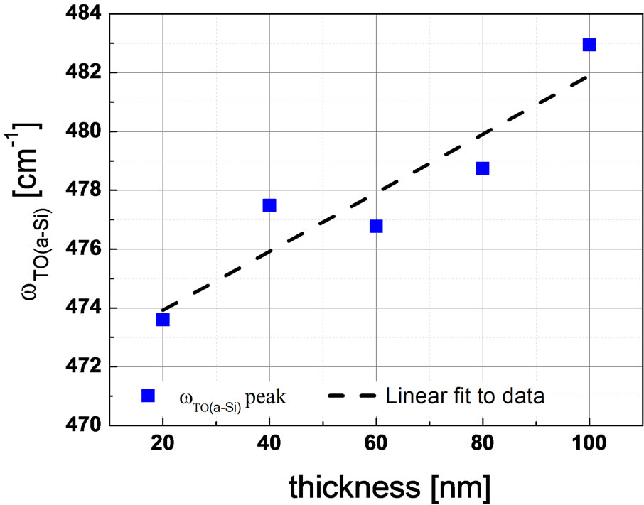
Figure 10. Variation of amorphous TO Raman peak ωTO(a-Si) on increasing p-doped silicon thin film thickness on glass substrate. The line serves as a guide to the eye.
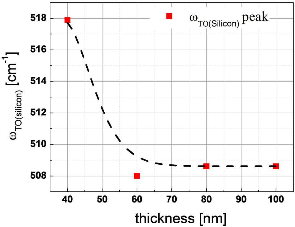
Figure 11. Variation of crystalline TO Raman peak ωTO(silicon) on increasing p-doped silicon thin film thickness on glass substrate. The line serves as a guide to the eye.
highlight that the deposited material is not homogenous in nature, and generally consists of a growth morphology of amorphous phase near the substrate towards an increasingly crystalline phase near the surface [41,42]. While our growing doped silicon thin film may experience structural relaxation, the level of structural relaxation at the amorphous phase near the substrate may not be the same as the microcrystalline phase near the surface, resulting in a higher tensile stress, as reflected from the Raman spectra. The resulting improvement in the conductivity of thicker films is not surprising due to the improved short range order as evident from the bond angle disorder reduction, improved film crystallinity, and expected improvement in doping efficiency.
Thus, in consideration of heterojunction silicon wafer solar cell device applications, the trend of thickness to crystallinity presents a trade-off between the low optical absorption of thinner doped films on one hand and better doping efficiency of thicker films on the other hand. For device application, the doped layer thickness should be around 10 to 20 nm, implying that further conductivity optimisation of the p-doped emitter layer is required to achieve both low optical absorption and high doping efficiency.
It is also relevant to highlight reports by Cabarrocas et al. [43], Fujiwara et al. [44], and Collins et al. [41] that the nucleation properties of doped microcrystalline silicon thin film are strongly dependent on the substrate. The comparison of film growth on different substrates, such as glass, crystalline silicon, as well as hydrogenated intrinsic amorphous silicon (a-Si:H) has shown different variation of film crystallinity with increasing thickness. To enhance μc-Si:H growth, it is reported that a hydrogen plasma pretreatment of the a-Si:H substrate can help to generate Si microcrystallites at the a-Si:H surface that act as initial nuclei for enhancing doped microcrystalline silicon thin film growth. We shall investigate this in the next section.
3.3. Influence of Substrate on Doped Silicon Thin Film Growth
In the heterojunction silicon wafer solar cell structure, the c-Si substrate is typically symmetrically passivated by intrinsic a-Si:H thin film layers (~5 nm) [19-22] before the deposition of the doped layers to establish the built-in potential requirements for charge separation and collection. In this section, we investigate the interaction of the deposited doped silicon thin film layers (~10 nm) on an intrinsic a-Si:H substrate at different hydrogen dilution ratios R = H2/SiH4. The a-Si:H(i) substrate is prepared by depositing a 5 nm a-Si:H(i) layer on microscopic glass substrates (1 mm).
Figure 12 shows a plot of the corresponding Raman spectra for p-doped silicon thin film (~10 nm) on an in-
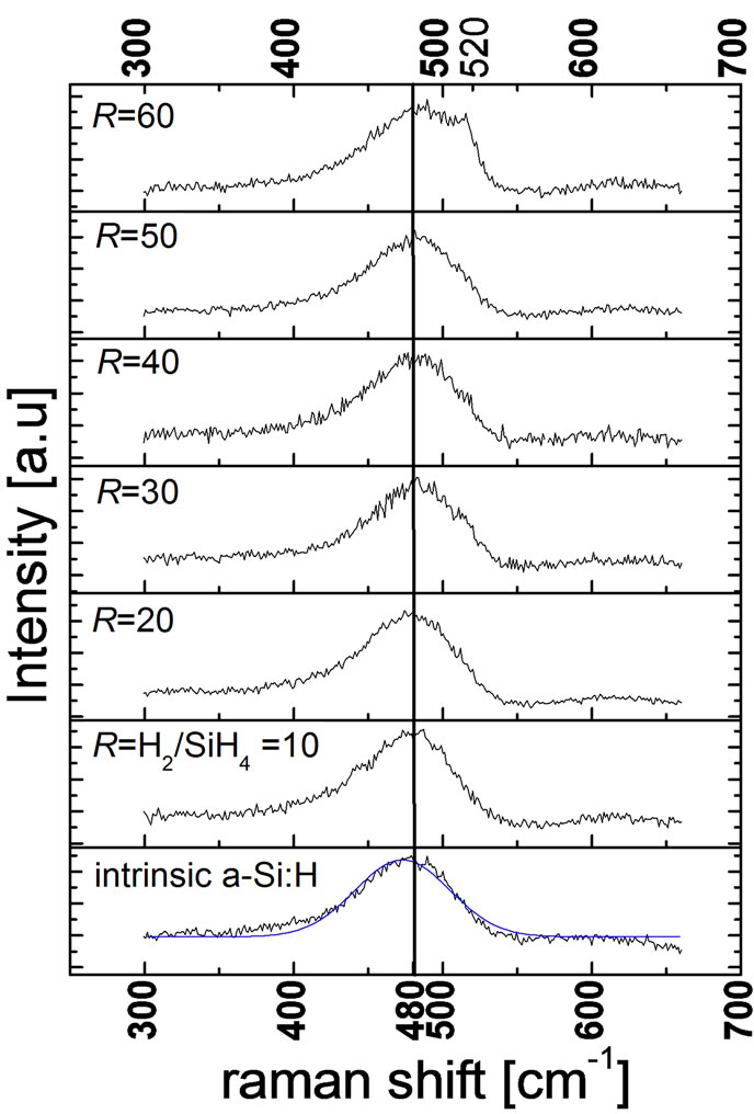
Figure 12. Comparison of the Raman spectra for borondoped silicon thin film (~10 nm) with different hydrogen dilution ratio R = H2/SiH4 deposited on thin intrinsic a-Si:H (5 nm) layer on glass substrate.
trinsic a-Si:H substrate. For the case of the intrinsic a-Si:H on glass sample, the a-Si peak position frequency is noted as 474 cm−1, a linewidth ГTO(a-Si) of 74.5 cm−1, and a dominantly amorphous structure (χc = 0.16%). By depositing the p-doped silicon thin film (~10 nm) with increasing hydrogen dilution ratio on the intrinsic a-Si:H substrate, a gradual shift in the Raman spectra towards higher frequency is observed. For the case of very high dilution ratio R = 60, the crystalline TO peak position can be observed (see Figure 13) where the deconvolution of the Raman spectra shows that the amorphous silicon peak position frequency, its line-width, and crystallinity can be extracted as 475.7 cm−1, 65 cm−1, and 15% respectively.
Figure 14 shows that while the intrinsic a-Si:H alone shows a rather high bond angle disorder of 9.90, the deconvoluted Raman spectra of the combined a-Si:H(p)/ a-Si:H(i) stack shows a reduced bond angle disorder regardless of the hydrogen dilution ratio. With increasing hydrogen dilution ratios, we observe a general reduction in the bond angle disorder, coupled with increasing film crystallinity (see Figure 15). From this experiment series, the role of hydrogen during deposition of a doped layer on an a-Si:H(i) substrate is clearly evident, whereby a higher H flow promotes both p-doped microcrystalline thin film growth, and reduces the combined network strain, hence lowering bond angle disorder. This finding is in line with reports by Kail et al. [45] and Chakraborty et al. [46] in which the annealing temperatures experi-
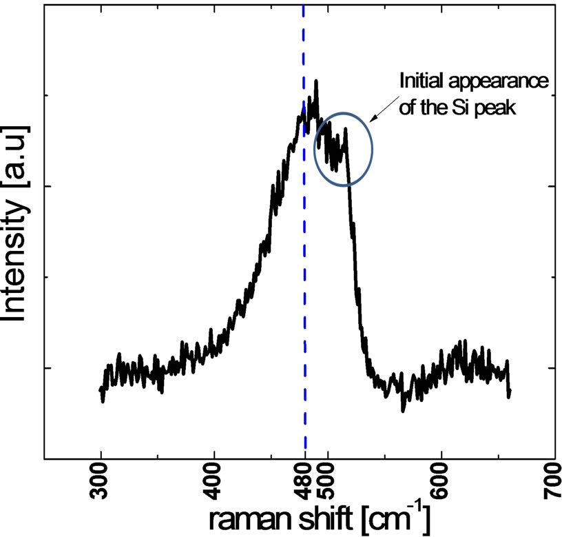
Figure 13. Raman spectra corresponding to the hydrogen dilution ratio R = 60 of boron-doped silicon thin film (~10 nm) deposited on thin intrinsic a-Si:H (5 nm) layer on glass substrate.
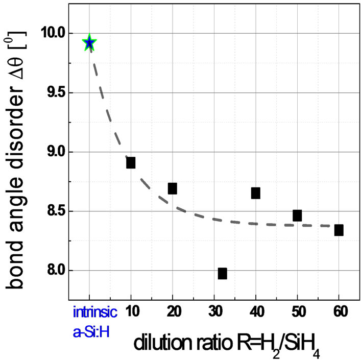
Figure 14. Impact of hydrogen dilution ratio R on bond angle disorder Δθ for boron-doped silicon thin film (~10 nm) deposited on thin intrinsic a-Si:H (5 nm) layer. The squares refer to the boron doped silicon thin film on intrinsic a-Si:H layer on glass. The star refer to that of thin intrinsic a-Si:H layer on glass substrate only.
ment on hydrogenated a-Si:H(i) samples have shown increased bond angle disorder with increased annealing temperatures due to dehydrogenation of the a-Si:H(i) samples. The hydrogen radicals can also potentially diffuse through the intrinsic buffer layer to reach the c-Si/ a-Si:H(i) interface for further passivation. Simulation studies in Section 3.5 will confirm this hypothesis using the measured effective lifetime curves of heterojunction lifetime structure [p/i/c-Si(n)/i/p] from Section 3.4.
At low H dilution ratio R = 10, the combined film crystallinity indicates low impact on the underlying intrinsic a-Si:H substrate, but the deposited doped silicon thin film experiences more short range disorder as
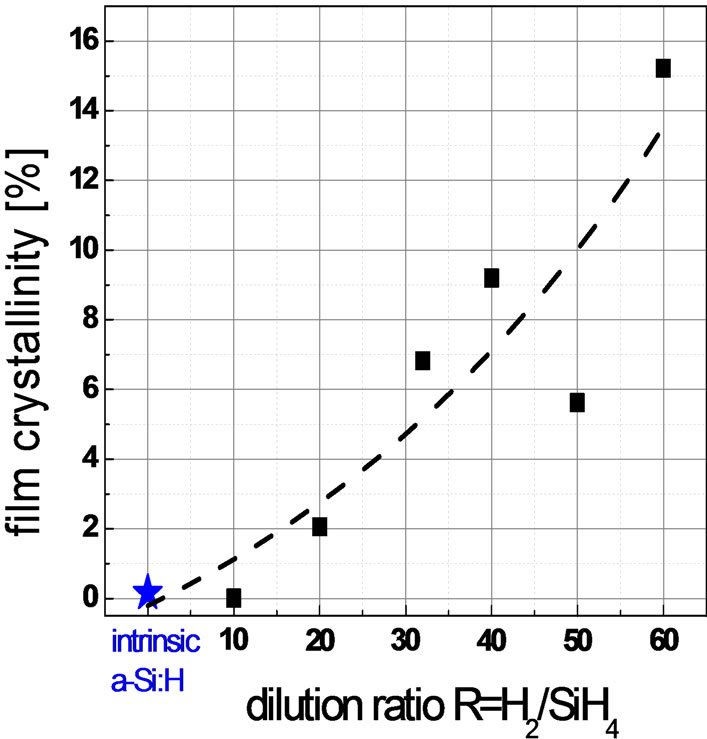
Figure 15. Impact of hydrogen dilution ratio R on film crystallinity % for boron-doped silicon thin film (~10 nm) deposited on thin intrinsic a-Si:H (5 nm) layer. The squares refer to the boron doped silicon thin film on intrinsic a-Si:H layer on glass. The star refer to that of thin intrinsic a-Si:H layer on glass substrate only.
evident from the higher Δθ. At very high H dilution ratio R = 60, the high density of the plasma hydrogen radicals can lead to increased etching action, and degrade the underlying intrinsic buffer layer. In perspective, depositing the p-doped silicon thin film with H dilution ratio R in the range of 20 - 30 on the intrinsic a-Si:H buffer might be a way to compromise between minimising the damage to the intrinsic buffer layer, while striving towards a microcrystalline doped silicon thin film with higher doping efficiency for solar cell application.
3.4. Device Relevant Heterojunction Silicon Wafer Lifetime/Solar Cell Structure
To assess the suitability of the doped silicon thin film layers for heterojunction silicon wafer solar cell application, we fabricated firstly a symmetrically passivated heterojunction carrier lifetime sample with the structure p+/i/c-Si(n)/i/p+, as illustrated in the inset of Figure 16, and secondly a heterojunction solar cell structure p+/i/cSi(n)/i/n+, while comparing with the i/c-Si(n)/i structure. The chosen thickness for the intrinsic (i) layer and the p-doped layer for the carrier lifetime structure in Figure 16 are 10 and 20 nm, respectively. The chosen thickness for the intrinsic (i) layer, p-doped and n-doped layer on the solar cell structure are 5, 20 and 20 nm respectively. The p-doped silicon thin film is deposited with a H dilution ratio of 32, and B2H6 = 2.2 sccm, while the n-doped silicon thin film is deposited with a H dilution ratio of 30, and PH3 = 2 sccm based on the analysis from earlier sections.
Over here, we demonstrate that both of our heterojunction structures showed improved minority carrier
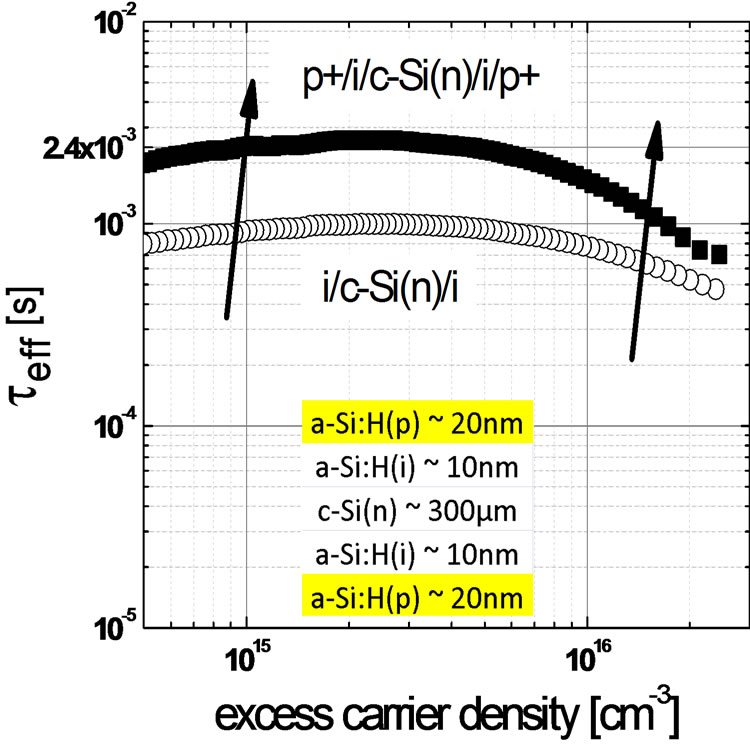
Figure 16. Effective carrier lifetime of bifacial heterojunction structure with symmetrically passivated intrinsic aSi:H layers only (open-circles) and complete layer stack (closed-squares). Improvement in the overall lifetime with the symmetrical p-doped silicon thin film layers is observed. A high minority carrier lifetime of 2.4 ms is obtained at a carrier injection level of 1015 cm−3 for the heterojunction carrier lifetime structure p+/i/c-Si(n)/i/p+.
lifetimes across all injection levels of interest as compared to the i/c-Si(n)/i structure alone. Understanding that the deposition process window for device quality doped silicon thin film is actually quite narrow, and with careful optimisation, it is possible to achieve a high degree of heterojunction interface passivation with the developed doped silicon thin films in this work. In particular, the heterojunction carrier lifetime structure p+/i/cSi(n)/i/p+ in Figure 16 shows an improvement from 0.9 ms (i/c-Si(n)/i) to 2.4 ms at the minority carrier injection level of 1015 cm−3, and a corresponding implied opencircuit voltage of 725 mV (Figure 17).
On the other hand, the heterojunction solar cell structure p+/i/c-Si(n)/i/n+ has a much thinner intrinsic a-Si:H layer (~5 nm), and the structure of i/c-Si(n)/i gave a significantly lower minority carrier lifetime of 31 μs at the injection level of 1015 cm−3, and a lower implied open circuit voltage at 550 mV (Figure 18). This is commonly reported to be due to reduced passivation quality by very thin intrinsic a-Si:H layers. Nonetheless, we demonstrate over here that with the application of the p-doped and n-doped layers, there is substantial improvement in the implied open circuit voltage by ~100 mV to reach 650 mV, and minority carrier lifetime improved from 31 μs to 390 μs which is expected to arise from efficient field effect passivation complementing the chemical passivation by the intrinsic a-Si:H layers on the c-Si substrate. By the optimisation of the doping gas flow, and the hydrogen dilution ratio, it is possible to obtain doped silicon thin films with high conductivity, improved short range order, and reduced tensile stress for application in
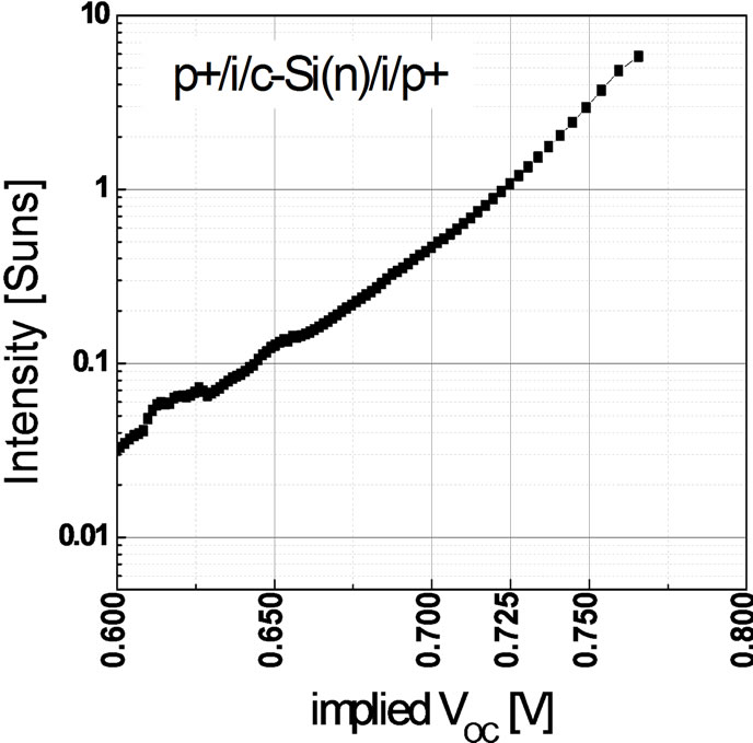
Figure 17. Implied Voc of the bifacial heterojunction lifetime structure as a function of intensity. The implied Voc at 1 sun is 725 mV.
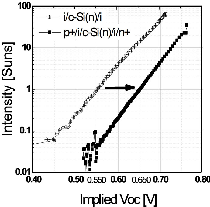
Figure 18. Implied Voc of the heterojunction solar cell structure. An improvement of ~100mV in implied Voc is observed upon application of the p-doped and n-doped silicon thin film layers. The implied Voc at 1 sun for the solar cell structure p+/i/c-Si(n)/i/n+ is 650 mV. The corresponding minority carrier lifetime improves by a factor of ~12 times at the injection level of 1015 cm−3.
a heterojunction silicon wafer solar cell.
Although we have limited samples showing the correlation of hydrogen dilution ratio or doping flow on stacked effective lifetimes, we are still able to predict degraded effective lifetime characteristics with higher hydrogen dilution ratio or doping flow based on earlier discussions. Deviation from the optimum deposition condition can lead to degraded interface quality and lower solar cell efficiency which is part of our simulated investigations in the next section.
3.5. Simulation Studies of Injection Dependent Effective Lifetime Curves
There are various reports related to the calibration of amorphous silicon thin films bulk properties and c-Si/ a-Si:H(i) interface properties [47-51] for the heterojunction silicon wafer solar cell. In particular, Rahmouni et al. [50] has calibrated the simulation input parameters for a-Si:H(p), a-Si:H(n), a-Si:H(i), and interface properties with the c-Si substrate to match with measured results from Taguchi et al. [52]. Using Ref [50] as a starting point, a similar calibration has been established with Sentaurus TCAD as well (See Figure 19 for a schematic of the solar cell and Table 3 for the comparison of our simulated and experimental cell performance). A consistent set of models and parameters for the simulation of Silicon solar cells were adopted [53], including FermiDirac statistics, Klaassen’s unified mobility model, radiative/Auger recombination, and its temperature dependence. Next, we perform the calibration of the bulk and interface properties of our in-house developed doped silicon thin film layers using injection dependent effective lifetime curves of symmetrically passivated n-type c-Si wafers. Figure 20 shows the resulting fit of measured data for both [i/c-Si/i] and [p/i/c-Si/i/p] lifetime structures. Table 4 shows the extracted interface properties.
For an unpassivated silicon wafer, the interface defect density Dit is reported to be approximately 1013 cm−2∙eV−1 [54]. We define the c-Si(n)/a-Si:H(i) interface defect distribution as two Gaussian distribution centered around midgap with a correlation energy of 0.2 eV. While the application of the a-Si:H(i) buffer layer with device relevant thickness (~10 nm) has reduced Dit to 4.6 × 1012 cm−2∙eV−1, we show in Table 4 that the further addition of the a-Si:H(p+) thin film layer (~20 nm) and subsequent H annealing at ~180˚C is able to significantly reduce Dit to ~5 × 1010 cm−2∙eV−1. Even without the aid of simulation, the improvement in the interface quality can be predicted from the significantly higher effective carrier lifetime of 2.4 ms at the injection level of 1015 cm−3 for the [p/i/c-Si/i/p] lifetime structure as compared to [i/c-Si/i] of 0.9 ms. It is reasonable to assume a lower interface defect density or surface recombination velocity as a result of additional field effect passivation from the doped
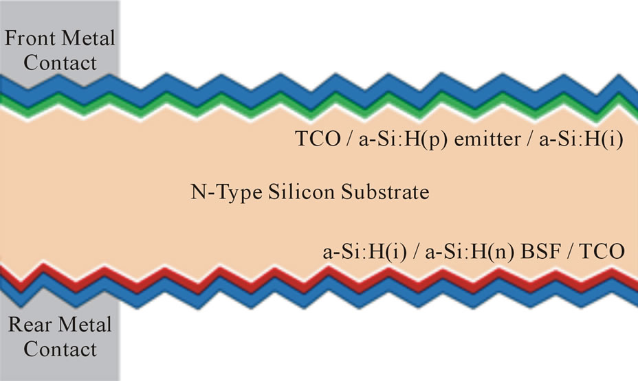
Figure 19. Schematic of a double heterojunction with intrinsic thin layer (HIT) structure.
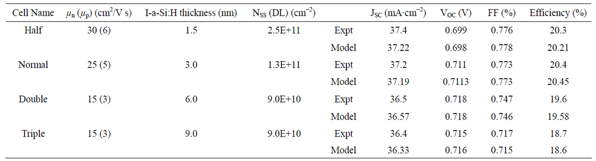
Table 3. Modeling of the measured cell performance parameters of double HIT structure solar cells on c-Si(n) substrate [52]. NSS (DL) is the interface defect density on either c-Si(n)/a-Si:H(i) interface.
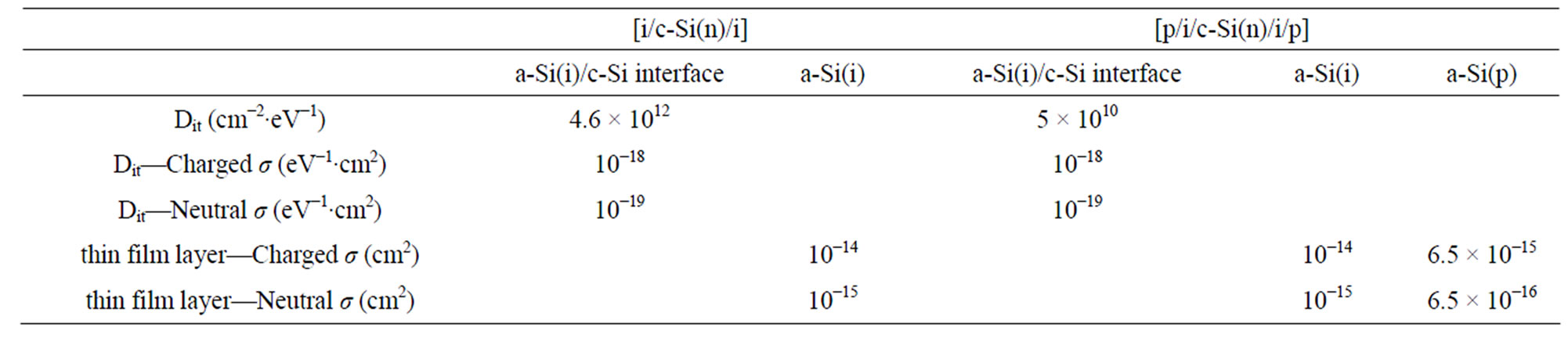
Table 4. Extracted interface defect distribution for both [i/c-Si(n)/i] and [p/i/c-Si(n)/i/p] lifetime structures deposited on n-type FZ wafers. The interface defect distribution is defined as two Gaussian distributions with correlation energy of 0.2 eV situated around midgap. A fitting of the Gaussian interface defect density Dit and capture cross sections σ is performed to obtain a decent fit to measured results in Figure 20.
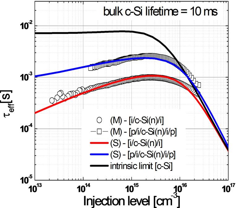
Figure 20. Fitting of the measured injection dependent minority carrier lifetime curves for [i/c-Si/i] and [p/i/c-Si/i/p] lifetime structures deposited on FZ wafer of resistivity ~3 ohm cm and 140 µm thick. Also included is the intrinsic limit of c-Si(n) substrate assuming a bulk lifetime of 10 ms and ideal surfaces (i.e.: Seff = 0 cm/s).
layers [48] as well as benefiting from the additional H annealing [55] typically applied after deposition of the doped layers in our work. If the interface defect density does not reduce with the application of doped layers, we would expect to see effective lifetime curves similar to Figure 21, where the effective lifetime at the same injection level of 1015 cm−3 would not see major improve-
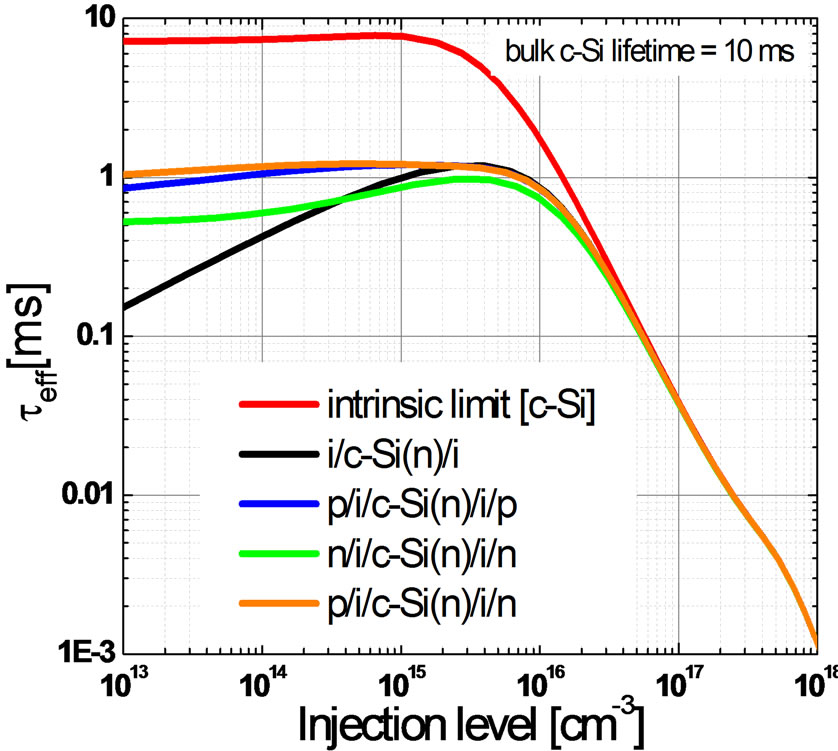
Figure 21. Simulated injection dependent effective lifetime curves of different stacked lifetime structures. Over here, the c-Si(n)/a-Si:H(i) interface defect density Dit is assumed to be invariant at 4.6 × 1012 cm−2∙eV−1 for all stacked lifetime structures. The application of doped silicon thin film layers provides field effect passivation, evident from the improved effective lifetimes at low injection levels as compared to [i/c-Si(n)/i] structure alone. The c-Si(n) substrate is assumed to have a bulk lifetime of 10 ms and with only single midgap traps.
ments, although at low injection levels, the minority carriers lifetime are higher than [i/c-Si(n)/i] structures benefitting from field effect passivation.
Hence, the choice of the deposition conditions for the doped silicon thin film layers affects not only the bulk doped thin film properties, it can also have a direct impact on the interface defect density and passivation quality. Figure 22 evaluates the impact of increasing interface defect density Dit on the injection dependent effective lifetime curves of [i/c-Si(n)/i] structures.
From Figure 22, the most significant impact of increasing Dit is the decrease of effective lifetimes at low injection levels. This has an important implication on the cell performance during low or medium incident light levels where the lower minority carrier lifetime is associated with lower diffusion length, and corresponding lower collection efficiency at the contacts. However at high injection regions, there is practically no difference in the curves as Auger recombination dominates in this region. We also observe from simulation that the bulk of the Auger recombination takes place near the front emitter and back surface field regions, since most of the photogeneration occurs near the front surface, while the back surface field regions is associated with charge collections. The lower injection levels is then associated mainly in the bulk region, where the minority carriers to be collected should have a sufficiently high diffusion lengths in order to have a higher probability of collection before recombination takes place. Table 5 shows a direct impact of varying Dit on the cell performance. Improving Dit directly improves all key cell parameters (short circuit current density JSC, open-circuit voltage VOC and fill factor) bringing immediate cell efficiency gains from 20.7% at a Dit of 5.5 × 1011 cm−2∙eV−1 to 22.5% for a Dit of 5 × 1010 cm−2∙eV−1, a relative gain of 8%. Having such a low Dit is achievable as demonstrated in our own lifetime structures, and highlights the importance of the doped thin film optimisation process. For a less than optimum doped layer, a higher Dit is expected, and lower cell efficiencies will result.
4. Conclusions
In this paper, we report the application of μ-Raman spectroscopy on the hydrogenated doped silicon thin film layers for application in crystalline-amorphous silicon heterojunction solar cells. Some key findings are summarised as follows:
1) With increase in doping gas flow, the film crystallinity is reduced due to low doping efficiency. Electrically inactive dopant atoms are likely to act as recombination centres and degrade solar cell performance. In addition, vibrational modes are getting more localised as observed from the shifts of the amorphous silicon TO
Figure 22. Impact of increasing interface defect density on effective lifetime curves for [i/c-Si/i] structure.
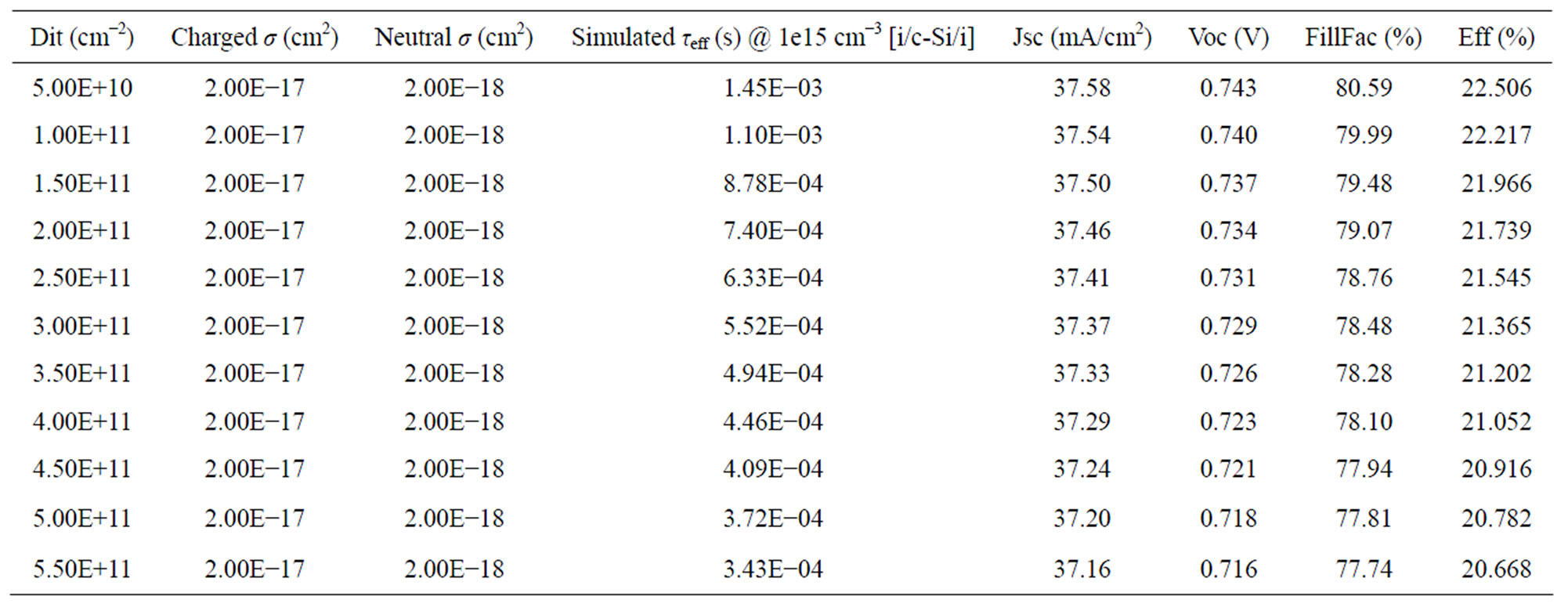
Table 5. Influence of c-Si/a-Si:H(i) interface defect density Dit on simulated injection dependent minority carrier lifetime curves and HIT solar cell performance. The heterojunction with thin intrinsic layer (HIT) cell consists of a [TCO/p+/i/c-Si(n)/ i/n+/TCO] structure. Improving Dit directly improves solar cell performance.
Raman peak to higher frequencies. The corresponding crystalline TO Raman peak downshifts to lower frequencies, indicating higher tensile stress in film.
2) With increasing film thickness, the film evolves from amorphous into microcrystalline phase with improved conductivity. We observed reduced bond angle disorder with thickness, believed to be due to structural relaxation. Amorphous silicon TO Raman peak also shifts to higher frequencies, indicative of reduced bond length. Increased tensile stress is also observed, subjected to the growth morphology of the silicon thin film.
3) Considering a stack of doped silicon thin film layer on intrinsic a-Si:H layer, reduced bond angle disorder is observed with increasing H dilution ratio, indicating improved short range order. The role of the hydrogen introduced during doped film deposition is expected to reduce strain, reduce weak Si-Si bonds, and enhance the nucleation for doped silicon thin film in the microcrystalline phase.
4) Combining our doped silicon thin film layers into different heterojunction structures has shown efficient field effect passivation and additional reduction in interface defect density, through improvement in minority carrier lifetimes across all injection levels of interest. With a thinner intrinsic a-Si:H layer, degradation in device lifetime is expected due to reduced passivation effects, but the addition of our doped silicon thin films has reduced the detrimental effects, evidenced by improvement in implied open-circuit voltage (~100mV). By the optimisation of the doping gas flow, and the hydrogen dilution ratio, it is possible to obtain doped microcrystalline silicon thin films with high conductivity, improved short range order, and reduced tensile stress for application in a heterojunction silicon wafer solar cell.
5) By simulating a HIT cell structure with our in-house developed silicon thin films, we demonstrate improvement in all cell performance parameters with improving interface defect density Dit, achievable with careful optimisation of the doped and intrinsic thin film deposition parameters. µ-Raman spectroscopy has been an essential tool in this work allowing us to obtain both quantitative and qualitative information about thin film bulk properties, as well as its interaction with underlying layers, allowing us to predict the performance of these developed thin films before integration into a solar cell structure.
5. Acknowledgements
SERIS is sponsored by the National University of Singapore (NUS) and Singapore’s National Research Foundation (NRF) through the Singapore Economic Development Board (EDB).
NOTES