1. Introduction
The composite a-nc-Si:H thin films have been the subject of intense research for a variety of applications due to their unique optical and electrical properties. Out of the many applications silicon thin films are used in thin layer transistors [1] , tunable photo-diodes [2] , and potential applications of composite silicon thin films are in third generation photovoltaic [3] [4] . First benefit of using a-nc-Si:H concerns optical properties. The optical gap of amorphous-nano-crystalline thin film materials can be adjusted in wide range with variation of size distribution of individual crystal sizes and the crystalline to amorphous fraction [5] . The nano-crystals remain as individual in amorphous matrix enabling quantum size effects related to small dimensions of crystals. Measurements of the optical properties and structural analysis in previous papers [6] showed that the spectral distribution of the absorption coefficient, in a wide range of crystal to amorphous fractions, can be maintained close to pure amorphous silicon in the visible part of the spectrum and showed square dependence on the photon energy. The average optical gap was larger for smaller nano-crystals and a higher crystal fraction Xc just confirming the quantum size effects that correspond to quantum dots [7] [8] .
Impedance spectroscopy has been widely used in the last couple of years as a powerful technique for the study of the dielectric and conductivity behavior of ferroelectrics, ceramics, crystalline bulk and compositecrystalline silicon thin films [9] -[11] .
Having in mind that silicon thin films samples are used in composite form, which is primarily characterized by the crystal fraction Xc and crystal grains sizes, it is necessary to understand effects of complex micro structural features on the overall electrical properties of thin films. The resistance and capacitance of crystals grains and grain boundaries, which is frequency and temperature dependent, can be evaluated from IS spectra. This technique for determination of the starting values for the basic equivalent electrical circuit was used in the fitting procedure of experimental impedance data with simulated data in order to select the most appropriate equivalent circuit. This technique enables us to separate the real and imaginary component of the complex impedance and related parameters, and hence provides information of the structure-property relationship in the rated samples.
The samples examined by IS technique with composite structures as silicon a-nc films with presence of crystals grains and grain boundaries embedded in matrix demonstrate complex impedance common in the event of two phase materials with different conductivity or permittivity. At high temperatures may occur two successive semicircle arcs mostly as a rule. These properties can conventionally be displayed in a complex plane plots (Nyquist diagram) in terms of the same formalism [12] :
Complex impedance:
 (1)
(1)
where  and
and  with
with .
.
Complex admittance:
 (2)
(2)
Complex permittivity:
 (3)
(3)
Complex modulus:
 (4)
(4)
The relationship between them is given as
 ,
, (5a)
(5a)
And
 , (5b)
where omega is angular frequency ,
,  presents the capacitance of the measuring cell in vacuum without presence of sample where A is cell area and d is plate distance or sample thickness, respectively. Furthermore,
  is permittivity of free space
 .
.
The micro-structural properties revealed by techniques like grazing incidence X-ray diffraction (GIXRD) [5] , Raman spectroscopy (RS) or X-ray powder diffraction (XRD) are fundamental in composite silicon thin films investigations but the correlation between microstructure and electrical properties is not always obvious or straightforward. Electrical properties may vary in intrinsic material and are intensive to minor variations in structure and composition or whether the properties are extrinsic since they could vary dramatically if impurities are present, especially if impurities to the grain boundaries [13] . Thanks to impedance spectroscopy and appropriate data analysis it is possible to characterize the different electrically active regions in a material, qualitatively by demonstrating their existence and quantitatively, by measuring their individual electrical properties. Identification and adoption of the most appropriate equivalent circuit for representation of the electrical properties are essential as a further step towards proper understanding sample properties. It has to be done in materials that are electrically particularly heterogeneous and where the impedance response of one part of sample overlaps, in frequency domain, with the response of other regions, giving rise to a composite response. Therefore, from an equivalent circuit model analysis the responses of the different regions may then be deconvoluted and characterized separately. The adequate model subsumes that are acquired simulation results have to be consistent with experimental data. This is, in most cases, based on designers experience on various equivalent circuit modeling.
Experimental
Samples of amorphous and amorphous-nano-crystalline thin films with a thickness between 100 and 200 nm were deposited by the PECVD method using radio frequency glow discharge in a capacitively coupled parallel plate reactor, as described earlier (Gracin, Thin Solid Films). Two gas mixtures were used, one consisting of 5% silane and 95% hydrogen, for amorphous-nano-crystalline Si layer and other with 90% silane and 10% hydrogen for pure amorphous Si. The substrate was glass.
The High-Resolution Electron Microscopy (HRTEM) measurements were performed in a JEOL JEM-2010F transmission and scanning electron microscope (TEM/STEM). The size distribution was estimated after software image processing in the reciprocal space using Bragg masks in the Digital Micrographs software. The individual sizes of the nano-crystals were approximated as spheres with a circular projection [7] .
The electrical conductivity of the thin films was measured by impedance spectroscopy (Novocontrol Alpha-N dielectric analyzer) in the frequency range 0.01 Hz - 10 MHz and in the temperature range 170 - 400 K. For the electrical contact, two gold electrode pads separated by 4 mm were sputtered on the sample surface using SC7620 Sputter Coater, Quorum Technologies. The impedance spectra were analyzed by equivalent circuit modelling using the complex non-linear least squares fitting procedure.
2. Materials Characterization
First, Typical HRTEM micrograph of a-nc-Si sample after software image processing is given in Figure 1. The nano-crystals are isolated from each other and various shape and orientation. After statistics made on some 10 such micrographs, the distribution is obtained. The average size of crystals in samples was about 8 - 9 nm, whereas crystal size distribution was broad.
Distribution of isolated nano-crystals is plotted in Figure 2. The best mathematical fit to the data was lognormal distribution, which suggests random nucleation. The volume fraction of crystalline/amorphous phase, estimated from the ratio of integrated intensities under crystalline diffraction peaks and broad amorphous contributions, was about 30%. The average crystal size was estimated from the width of crystalline peaks using

Figure 1. Typical micrograph of a-nc-Si:H sample. The nano-crystals are assigned by lines for better visibility.
Scherrer formula assuming that the size broadening due to strain could be neglected comparing to the size broadening. In that way obtained values are the same as estimated from HRTEM micrographs just verifying the procedure.
Typical GIXRD diffraction patterns for measured samples are displayed in Figure 3. One can see crystalline silicon Bragg reflections 111, 220, 311 superimposed on the background features related to the amorphous silicon matrix.
The as deposited samples were heated in vacuum at 400˚C for one hour. The heated samples exhibited the same ratio between crystalline and amorphous fraction while position of crystal peaks was shifted towards higher angles for about 1% which implies that unit cells became smaller, possibly due to hydrogen evolution. In the same time, the width of spectral lines became larger. The explanation for increase of peak width could be decrease of crystal sizes and/or increase of strain. Hydrogen concentration during the heath treatment decrease from about 8 to 4 at %, as measured by ERDA which could change the strain in film.
3. Analysis of Improved Circuit Model
Impedance response of silicon composite thin films usually cannot be presented correctly by an ideal semicircle arc based on simple model of parallel RC elements. There are various approaches to model non-ideality of electronically and ionically conducting materials such as amorphous/crystalline materials. In man cases is useful to
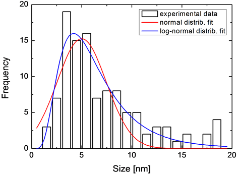
Figure 2. Typical size distribution of a-nc-Si:H sample. The lines represent mathematical fit to the data.
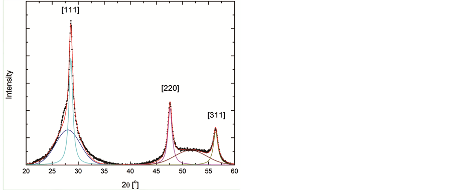
Figure 3. Typical GIXRD data of a-nc-Si:H thin film. The crystalline silicon Bragg reflections are highlighted.
use a combination of electrically active components together with constant phase elements, CPS, to represent the departures from Debey-like ideality [9] . The CPE describe the widely-observed power low dependence of the impedance components on frequency. Since non-ideality of impedance response in silicon samples are observed, introduction of CPS is mainly instead of ideal capacity used in previous modeling. Therefore, the admittance of modified complex equivalent circuit according to literature [12] is:
 . (6)
. (6)
And impedance is given by:
 . (7)
. (7)
Parameter A is a constant that is independent of frequency related to CPE capacitance, and n is an exponentional index that is measure of distortion of  characteristics. Parameter n is known as “non-ideality” Debey-like curve parameter. The other formalism like modulus can be generated readily by means of transformation (5a) and (5b) mentioned before.
Analysis of data yield in such possibly depressed arc will be considered in this part of paper. As shown in Figure 4 [12] , Rs and Rp are serial and parallel resistors included in simple equivalent circuit (Figure 4 right inset) with Rp in parallel with CPE element. Usually, in precise circuit analysis a serial resistor Rs is the uncompensated resistance of electrode leads and also resistance between the electrode surfaces in junction with surface of sample under investigation. Since its parameter is a few orders of magnitude less in comparison to composite sample DC resistance, its influence in numerical analysis can be negligible.
The relation between complex equivalent circuit parameters (Rp, n, Θ) according to curve parameters (x0, y, w, ωmax) in Figure 4 are:
 , (8)
, (8)
with transformation 
Opposite expression gives relation to non-ideality parameter n:
 . (9)
. (9)
Finally, derived from Figure 4 parallel resistance is .
.
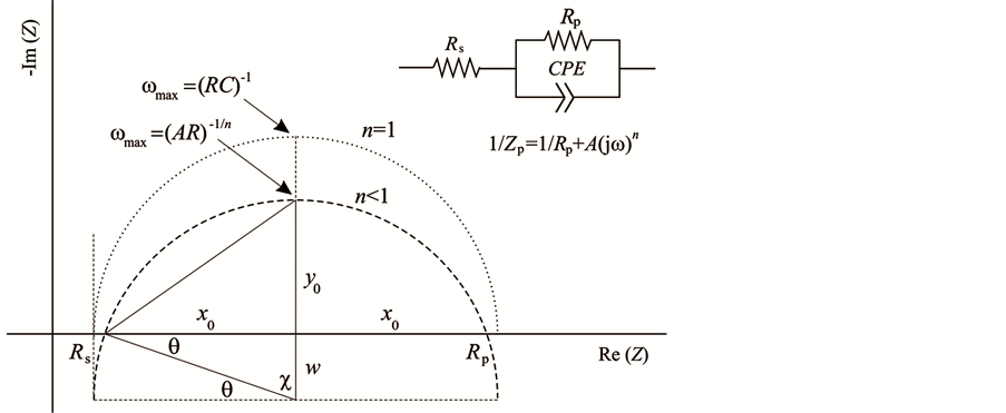
Figure 4. Impedance Z plane for a depressed circular arc shoving definitions of quantities used in numerical analysis.
For n = 0, CPE behaves like pure resistance with the value R = 1/A. Similarly, if n = 1, Θ = 0 and semicircle arc is ideal Debey-like curve.
More complex circuit model can be extracted from single Rp||CPE parallel element to two R1||CPE1 and R2||CPE2 parallel elements in serial connection as shown in Figure 5. In that case impedance data can be presented with two depressed arcs similar like in case with simple basic equivalent circuit consists of two parallel resistor capacitor (RC) elements. Therefore, modulus plot  and impedance plot
  do not coincides if sample temperature is not high enough and modulus peak shift toward higher frequencies could be expected.
4. Experimental Results and Discussion
Amorphous-nano-crystalline composite silicon thin films have been investigated in the frequency range 0.01 Hz - 10 MHz and in the temperature range 170 - 400 K. Experimental impedance data of samples shows semicircle arcs in tree temperature cases: 360 K, 380 K and 400 K, according to Figure 6 (right inset), respectively. Interpreting the results of IS experiment to give information on electrical properties (conductivity) or microstructure picture (existence of two phases), especially for complex materials like a-nc-Si:H requires a kind of complex and unusual approach.
Most experimental IS results are interpreted in terms of series or parallel combinations of resistors and capacitors and special elements like the CPE. Also, it is often incorrect to describe the complex topology of real microstructures only by using simple series and parallel ideas. Moreover, physically is not possible to consider the complex microstructure as either a parallel or a series arrangement of phases. Rather, since the current must flow through amorphous lower-conducting phase in some percolation effective path and through higher-conducting nano-crystalline phase, there is a degree of tortuosity present, which gives a more complicated IS response.
Therefore, inclusion geometry and crystal sizes and more likely log-normal distribution of nano-crystals also contributes to determining how many arcs will appear in the impedance spectrum, and not just materials series or parallel character, which usually cannot be defined for a complex microstructure. One could speculate that two or more arc behavior will be observed if one or more of the phases is discontinuous, as was the case in reach a-nc-Si:H composite silicon thin films.
For better analysis purposes, the Nyquist plot of the impedance curves of the samples investigated at temperature of 400 K are shown additionally in Figure 7. Parameter Rp, as equivalent circuit resistance can be easily extracted out of semicircle curve from experimental data shown in Figure 7. The total resistance of the circuit can easily be read from the curve, and it is  for each sample. The presented spectrum allows clearly determination only dominant resistance (amorphous phase) and that is
 . According to improved complex circuit model non-ideality curve parameters n1 and n2 can be evaluated thru fitting procedure, graphically or by numerical calculation extracted from experimental data. Based on peaks plots of
  and electric

Figure 5. Impedance Z plane of improved complex circuit model with R1||CPE1 and R2||CPE2 elements in serial connection.

Figure 6. Experimental impedance of sample G01 shows semicircle arcs in tree temperature case (right inset): 360 K (blue); 380 K (green) and 400 K (very small red circle).

Figure 7. Experimental AC impedance spectrum of a-nc-Si:H samples G01 and G21 in complex plane.
modulus  as a function of frequency (Figure 8) one can determine parameters from equivalent circuit constant
 , and capacitances A1 and A2, respectively [10] . The basic fitting procedure evaluation indicates that there is more than one dominant arc present at higher frequencies, and most probably many arcs, with the distribution of resonant frequencies. But only one arc can be evaluated as effective to the second phase electrical property.
All calculations based on experimental data and fitting curves on impedance and modulus data are shown in Table 1 and Table2 The frequency , corresponding to
  plot, gives the rated parameters from equivalent circuit condition
  [9] .
[9] .

Figure 8. Plot of the impedance curve (left) and electrical modulus as function of frequency of samples G01 and G21.
Table 1. Calculated values of modeled equivalent circuit elements extracted of experimental impedance data.
Table 2. Calculated values of modeled equivalent circuit elements extracted of experimental modulus data.
Experimental data for both silicon composite thin films samples at rated temperature 400 K shown in Figure 7 points to conclusion that one dominant component (R||CPE) forms the non-ideal shape or compressed semicircle arc. From theory point of view it could occur in two situations: 1) in two parallel R||CPE elements in serial connection, or 2) in two parallel R||CPE in parallel connection. In both cases, according to our experimental data one circuit is pre-dominant.
The G01 is as deposited sample while G21 and G01 represent the sample heated at 400˚C for one hour in vacuum. During heath treatment at lower temperature is expected the increase of ordering of amorphous phase. The heath treatment at higher temperature result in partially evolution of hydrogen from amorphous network which enable formation of larger units with density higher than average. The capacity of sphere is given by relation , where r is radius of sphere, while/and/are dielectric constants. If approximating the nano-crystals with sphere, the increase of capacity of nano-crystalline phase size could be related to increase of average size of each crystal unit. The increase of capacity of amorphous phase could be explained with formation of larger units with higher density caused by hydrogen evolution.
Both aspects of the impedance spectrum described above indicate that the phases within the composite are arranged to some extent in a series manner, despite parallel connection of electrodes. In other words, the microstructure under investigation has series character. Since the nano-crystalline phase is the most conductive phase in the microstructure, the series behavior implies, according to the usual models used to analyze IS, that the nano-crystalline phase is somehow partly disconnected or overlapping in reach volume fractions with amorphous phase in higher frequencies areas.
The Nyquist plot of the impedance curve of the sample G01 investigated at temperature of 400 K is shown in Figure 9. The data points clearly that there is more than one arc present at higher frequencies, and most probably many arcs, with the distribution of resonant frequencies. The biggest integral arc represents dominant amorphous phase presented by R2||CPE2 element and evaluated with data from Table 1, especially amorphous resistance R2 = 7.22 GΩ and amorphous capacitance C2 = 2.62 pF according to simple model and more precisely capacitance A2 = 3.1 pF according to improved circuit model. Exponent index n2 is calculated as 0.986.
Additional calculated capacitance A1 =16.1 pF (shown in Table 2) can be evaluated only according to improved circuit model and thru  and
and  plots. This capacitance suggests existence of second present phase: reach nano-crystalline phase. Its existence is previously evaluated thru volume fraction index Xc = 33% [14] [15] . Consequently this is not just one particular crystal size or distribution influence to overall capacitance. More precisely, this value represents effective capacitance of all nano-crystals embedded in 3D amorphous matrix. It is almost impossible to extract one individual effect or influence from experimental impedance curve overlapping with many arcs of resonant frequencies, presented thru model in Figure 9. Nanocrystalline phase calculated capacitance A1 = 16.1 pF of a-nc-Si:H sample G01 suggests parallel connection of individual crystals whit substantially higher capacity than amorphous phase (A2 = 3.1 pF).
Furthermore, lower capacitance of 15.4 pF of sample G21 suggests decrease of nano-crystals in parallel connection according to temperature applied annealing processes and hydrogen atom redistribution in weak dangling

Figure 9. Nyguist plot of the impedance curve of sample G01, solid line represents experimental data and dashed line suggests Maxwell-Wagner possible model of resonant frequencies of the nc-Si:H phase.
bonds crystal grain boundary regions and predictable structural change phenomena in composite silicon thin films described before.
Additional impedance analysis reveals higher resistance of samples G21 in comparison to as deposited sample G01. Its conductance are decreased from 13.85 μS∙cm−1 to 12.18 μS∙cm−1 mostly according to possible increase of strain or possibly crystal grain boundary quantum wells growing phenomena significantly more than because of decrease of the amorphous phase reactance.
Evidence can be observed in the non-ideality parameter n2 of amorphous phase, being lower than one, in range . Furthermore, the non-ideality parameter n1 of nano-crystalline phase lower then n2 in range
  highlights the capacitive nature of composite structure reach of nano-crystals embedded in amorphous matrix.
Influence of nano-crystalline microstructure to electrical properties of thin film also can be seen on the electrical modulus plot. This relationship is presented in Figure 10. Experimental data presented with solid lines points electrical modulus characteristic dependent on frequency and dashed lines Maxwell-Wagner model of possible resonant frequencies and overlapping arcs according to [16] . Angular frequency ω rises towards higher values at right side of Figure 10. Main characteristic of all a-nc-Si:H samples is high sensitivity to higher frequencies, which can be presented and modeled with many small semicircle arcs according to the microstructure influence and present nano-crystalline phase. Quantitative analysis of  and
and  plots focused to G01 sample exhibits better conductivity of G01 in comparison to other samples. Smaller arc in Figure 7 and superior arc on Figure 10 suggests higher conductivity of G01 sample according to crystalline volume fraction, which is in good agreement to micro-structural properties revealed by grazing incidence X-ray diffraction.
Figure 11 shows the modulus master curve of a-nc-Si:H sample G01 as characteristic response of both samples under investigation at temperature 400 K.
The full-width at a half-maximum (FWHM) of  versus
  do not change in the temperature range considered. It is also observed that the
  curve is not symmetric, implying a non-exponential behavior of the conductivity relaxation. Also, curve is gently inclined toward higher frequencies indicating more dynamically processes of the conductivity relaxation at higher frequencies. The FWHM of the
  spectra (1.97 decade) is the same as the breath of a Debey peak
  (1.96 decade), which suggests the presence of Debey type of relaxation phenomenon [10] . Furthermore, according to Figure 11 at
  plot the frequency region below peak maximum (
 left curve side) determines the range in which free charge carriers are mobile on ”long distance”. Consequently, at frequency above peak maximum (
 right curve side), the free charge carriers are confined to potential wells (boundary of nano-crystals), and therefore are mobile on ”short distance” [17] [18] . Indication of small peak in that region suggests beginning of formation of second electrical modulus peak which could be better seen on temperatures higher than 400 K.

Figure 10. Nyguist plot of the electric modulus curve of two samples, solid line represents experimental data and dashed lines Maxwell-Wagner based overlapping arcs.
Figure 12 shows the specific DC conductivity  versus 1000/T plot of sample G01 at different temperatures extracted from IS data. It indicates pattern in which conductivity increases gradually with rise in temperature suggesting a thermally activated process in investigated material.
Activation energies Ea evaluated from the slope of the linear portion of the conductivity plots according to Arrhenius law are 0.71 ± 0.01 eV for amorphous phase and 0.51 ± 0.01 eV for nano-crystalline phase. The value of specific DC conductivity has been calculated from the admittance data using relation , where
  is the measured sample resistance, t is sample thickness (100 nm) and A sample area under investigation. Evaluated activation energies are difference between bottom of conductive band and Fermi level. If the Fermi level is at the middle of the band-gap, the mobility band gap of nc-Si:H phase is around 1.02 ± 0.02 eV, and the mobility bandgap of a-Si:H phase is around 1.42 ± 0.02 eV, which is close to expected optical band gap of crystalline and amorphous phase, respectively.
5. Conclusions
The AC impedance of amorphous-nano-crystalline silicon composite thin was studied in a wide frequency range at different temperatures. The impedance response of a-nc-Si:H samples were interpreted in terms of improved model of equivalent circuit with two parallel Rp||CPE connected in serial. By the analysis of equivalent circuit

Figure 11. Characteristic of dielectric modulus; master curve of a-nc-Si:H sample G01 at temperature 400 K.

Figure 12. Variation of specific DC conductivity of the sample G01 as a function of temperature.
impedance, combined with the analysis of experimental data of electrical modulus, it was possible to extract the resistance and capacitance contribution of amorphous and nano-crystalline regions to the overall electrical properties of silicon composite thin films.
More complex improved model of equivalent circuit is established in the fitting process of experimental impedance data. Multi-arc behavior of experimental results had proved presumption of multi-phase existence, series arrangement of dominant amorphous and nano-crystalline phase. The non-ideality parameter , being lower than one,
  highlights the capacitive nature of composite structure reach of nano-crystals embedded in amorphous matrix. The amorphous phase resistance is higher than the same of nano-crystals. Debey peaks observed in the plots correspond to relaxation process. Impedance peak against frequency is proportional to the resistance of the composite material, while the peak of electrical modulus against frequency is inversely proportional to the capacitance, determining equivalent circuit parameters.
AC impedance spectroscopy data confirm previous applied structural techniques on the composite silicon thin films and reveal fine resistance and capacity increase in amorphous phase after heat treatment due to hydrogen evolution and straight ordered domains. Also IS data reveal gentle decrease of capacity of nano-crystalline phase after heat treatment according to expected decrease of crystal size.
The Maxwell-Wagner equations do not work well for the overall impedance curve in the case of overlapping arcs because it cannot take into account overlapping the electrical capacitances presented with rich nano-crystals with possible tunneling effect. This appearance leads to effective percolation behavior of free carriers with possibly not percolation threshold instead. Calculated capacities of nano-crystalline phase represents effective values applied in investigating the crystal structure of nc-Si:H regardless of crystal series or parallel combinations.
Acknowledgements
The author would like to acknowledge Davor Gracin Ph.D. senior research adviser from the National Institute Ruđer Bošković a head of Photovoltaic group in Materials science department especially for his courtesy, research guidance and for comments that help improve the manuscript.